Other Parts Discussed in Thread: TI-JESD204-IP, , ADS54J60, LMK04828, ADS54J20
Hello TI,
A few days ago I contacted TI and received the TI-JESD204-IP (Rapid Design IP). I have modified the generic RXTX loopback example to enable ZCU102 receive data from ADS54J60EVM through the J4 HPC1 FMC connector. My desired config is the following:
ADC device: TI ADS54J60EVM (Rev. D)
JESD204 mode: JESD204b in subclass 1 mode
LMFS = 2221 in 4X decimation mode
K = 16 (frames per multiframe)
Sampling clock: 1Ghz. Logic clock: 250Mhz
Data bits per lane: 16
Line rate: 5Gbps
LMFC for mode 2221/4X → LMFC = (fs / 4) / K = (1000 / 4) / 16 = 15.625Mhz
SYSREF = LMFC / 8 → SYSREF = 1.953125Mhz
I am still facing issues with the ADC/TI-JESD204-IP setup. I would be very grateful if you could answer the following questions.
1. Does the provided TI Rapid IP support 16bit data lane width? If not, will I have to only use the 16 least significant bits in the normal 32bit data lane width mode?
2. Should I use the LMK config "LMK_Config_Onboard_1024_MSPS.cfg" and ADC config "ADS54J60_4x_dec_3Fs_16_2221.cfg"? My frequencies of interest are in the range of 170Mhz-200Mhz.
3. How should I set the desired SYSREF frequency in the ADS54Jxx GUI?
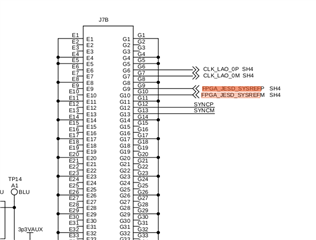
4. What are the necessary FMC pins that I should specify constraints for in my design? For example, FMC pins G9 & G10 (that are supposed to be SYSREF inputs for the JESD204b of the ADC module) are named as "FPGA_JESD_SYSREFP" and "FPGA_JESD_SYSREFN" in the ADS54J60EVM Rev. D schematic. Aren't these differential signals supposed to come directly from the LMK04828? And how the SYSREF signal is sourced to the ZCU102 "rx_sysref" input?
Thank you.