This thread has been locked.

If you have a related question, please click the "Ask a related question" button in the top right corner. The newly created question will be automatically linked to this question.

DAC8718 problem

Other Parts Discussed in Thread: DAC8718

Hi

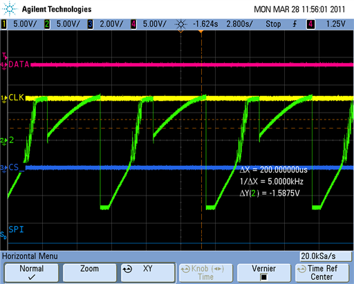
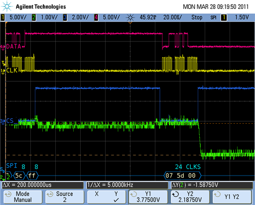
I have a problem with the DAC8718  converter: I can't get a correct output. The 2nd (green) channel in a picture below is a DAC output formed by sending a state of  16bit counter to the DAC broadcast register from 0000h to FFFFh. DAC is powered with +-12V source and reference if 4.096V.

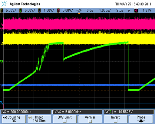
I expected to get a sawtooth style voltage from -12V to +12V with saturations. But the result I have got is far from the desired result. It starts from about -12V as expected but finishes at about +7.5V and the voltage shape is not linear.

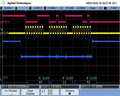
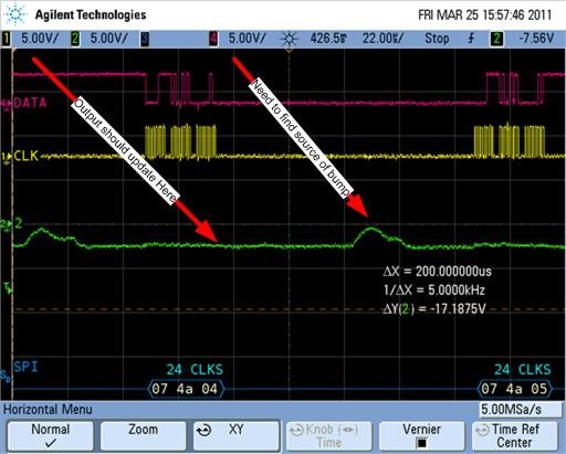
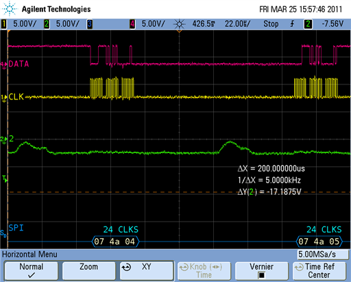
The next picture shows an excange with DAC. The result of sending 23C0h and 23C1h codes is about -9.7V output.

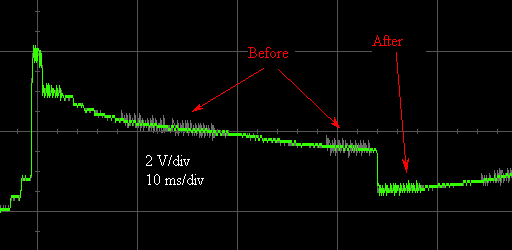
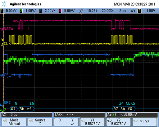
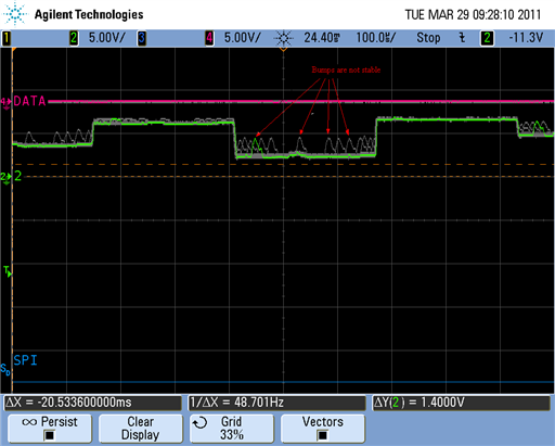
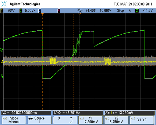
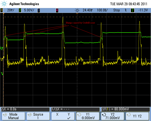
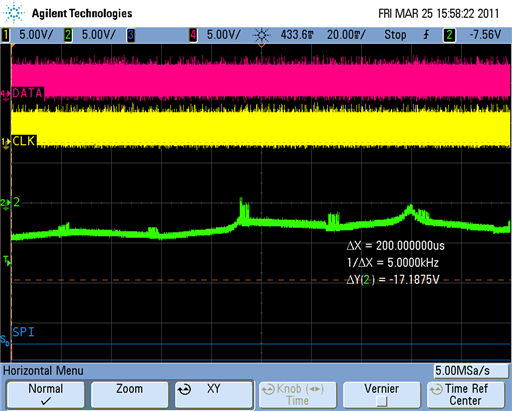
 The next few pictures show the most strange sections of the voltage shape.


 May be somebody knows how can I obtain a normal operation of this converter?

Thanks.


  • Hi Roman,

    We have not seen this behavior in the past. First thing I generally would have you do is check to make sure your timing signals are not violating and data sheet specs and you are using the falling edge of SCLK as the critical edge. It looks like you are able to communicate with the DAC problem free, it is just that the output looks 'unstable.' Could you post a schematic of your system that you are using for this test. It would also help if you could let us know the state of your static pins and your configuration register settings. Have you checked to make sure that your reference voltage is not having any problems? Is this behavior repeatable every time that you go to step up your codes to ramp the output?

    Regards,

    Tony Calabria

  • Hi Tony,

     This is my simplified schematic

    The reset pin is sourced by global board reset signal. The DAC's outputs are now unconnected. I've tried different combinations of RSTSEL and USB/BTC signals so some of scope pictures may be with USB/BTC tied low. LDAC connected to the DSC IO pin and now continuously low. 


    The more detailed timing diagram for SPI is below.

    The CLK signal frequency is about 1MHz. I think SPI timing far from the data sheet specs limit values.

    I don't send any data to  configuration register now. Earlier I was writing 0 to  configuration register. The result is same.

    The changes of the reference measuared with my oscilloscope are in 4.110V ... 4.116V so I think reference voltage is stable.

    The voltage on the OffsetA pin is 3.118V and on the OffsetB pin is 3.070V

    According repeatablity. At first sight it looks the repeatability of the DAC output behavior is very good.

     But with infinity persistence I have found some "thin structures" on the signal shape wich positions are moved.

     May be it is noise I don't know. The "main" shape of the output signal is repeated very good.

    Also the  output signal changes greatly when the low byte changes from 0xff to 0x00.


     Thanks,

    Roman Ermakov


  • Hi Roman,

    A couple comments / things I have noticed as I looked through your pictures.

    - You schematic - I did notice that you do not have the DGND in your schematic and I just wanted to make sure that you have that grounded and connected to AGND. You do not want to have the AGND and DGND connected on separate lines or separate planes as there is an internal diode to the DAC connecting the two GNDs together.

    - OFFSET DACs - Are your writing to set the offset DACs to some value other than the default reading? The reason I ask is by default, with a 4.096V reference, the offset DACs should read 2.457V (in a gain of 6) or 2.73V (in a gain of 4). Additionally, I did notice a fair amount of disparity between the readings from the two DACs. The offset DACs are 16 bit DACs and at a 16 bit level, I would expect the output voltages of those two DACs to be better matched. A 40mV difference is quite substantial.

    - I am unsure of the gain that you are running but from you scope pictures. My guess is that you are using a gain of 6 but you have a situation where the output range is only from -12V to +7.5V. It looks like the DAC is trying to output less than -12V but is clipping due to the power supplies required headroom. This may be due to your DACs set to a point where you are offsetting your output voltage so that it is clipping near the bottom rail. This does not really have anything to do with your output behavior you see but it is a FYI. Try and bumping up the power supplies to +/-15V to avoid clipping so you can utilize the entire code range.

    - Your most recent pictures that show the behavior is repeatable show make it look as if there is a certain code range that this occurs at. Could you find the code range. I need to try and see if I can repeat this in our lab to take a deeper look. Also, is the load on your output that you are driving?

    - Could you get a scope picture showing the reference voltage during the abnormal behavior. I would just like to make sure there is not a stability issue with the reference.

    - It looks like you are using the broadcast command 0x07xxxx to write to the DACs. Out of curiousity, have you tried to use a different command such as 0x08xxxx and update just channel 0. If not, could you try that and let me know what you see.

    Thanks,

    Tony Calabria


  • Hi Roman,

    One last test I thought of which would help narrow down this problem -

     - Rather than stepping up by single codes, could you step up in sets of 10 or 20 codes. This way I can see where the output step is updating in comparison to where we see the output bump or glitch. I posted a picture below to help explain what I am looking for -

    Let me know if this does not make sense.

    Regards,

    Tony Calabria

  • Hi Tony,

    Thank you for your attention.

    I have not separated DGND and AGND nets in my design. The ground net is called  GND and I have connected all 7 AGND and DGND pins to this net.

    My simple test program just sends a 0x07 byte and two counter bytes to the DAC so I don't  set other registers instead of the broadcast register. So I don't try to set offset DACs. May be they are updated for some inexplicable reason. I just measure voltages on the OffsetA and OffsetB pins with my oscilloscope.  The accuracy of the oscilloscope is not excellent. Tomorrow I will make more accurate measurements and let you know. Also I don't change control register so the gain must be 6.

    I understand -12V clipping reason but I don't understand +7.5V upper limit and  nonlinear and nonmonotonic character of transfer function.  In my design I really need a +-10V range. I have not any load on the DAC outputs now. I have removed R35 ... R42 resistors and made my measurements on the free DAC outputs. But I tried to connect 1KOhm resistor between the DAC output and GND for several times. There was no change.

    I think I need to number my pictures :) What picture do you mean? If it is the second one after the schematic then the code range is 0 ... 65535 and repeated 3 times. If it is the third one then I am afraid I cant find a code range relating to this picture but tomorrow I will make a new one and will find the code range for it. I think it does not really matter what place in the output waveform I will take.   

    I will try to make a reference voltage scope picture but  today I have measured the only 6 mV deviation of this signal. The most sensitivity oscilloscope's limit is 20mV/div and I suppose the resulting picture will be very close to a straight line.

    I have already tried updating of the only one channel. The result is the same. I will repeat it tomorrow, may be something will be changed. Also I think I need to compare different outputs at the same time.

    Regards,

    Roman Ermakov.


  • Hi Tony,

    I just receive your post.

    I've been supposed with such behavior too. Furthermore I have seen a bump during SPI activity (during CS is low).

    I can perform the test you ask tomorrow.

    Thanks,

    Regards,

    Roman Ermakov.

  • Hi Tony,

    I've found a source of the blumps.

    First of all the blumps are not stable. They are moves slowly over all scope so they  are not caused by the SPI exchange.   


    Figure 1.

    During mesuaring OffsetA and OffsetB pins in AC mode I detect some  slowly moved noise.

     Figure 2.

    This noise is the reason of the blumps or the blumps and the noise on the Offset outputs have same source.

    Figure 3.

    I need little more time to process my other results.

    Regards,

    Roman Ermakov.


  • Hi Tony,

    I have attached a PDF with oscillograms and comments for you. Also I have attached an archive with the source and addition pictures.

     2234.DAC8718pics.pdf

    5314.DAC8718pics.zip

    Today I worked basically with the 5th DAC channel (0th channel resistor is on the bottom side of the board and it is not useful to connect probe to it).

    The big noise (up to 80 mV) on the Offset outputs explains the poor matches of this signals.

    Also I implement Input Data and DAC Data registers reading. Both registers contain correct information.

    Regards,

    Roman Ermakov.