A related question is a question created from another question. When the related question is created, it will be automatically linked to the original question.
If you have a related question, please click the "Ask a related question" button in the top right corner. The newly created question will be automatically linked to this question.
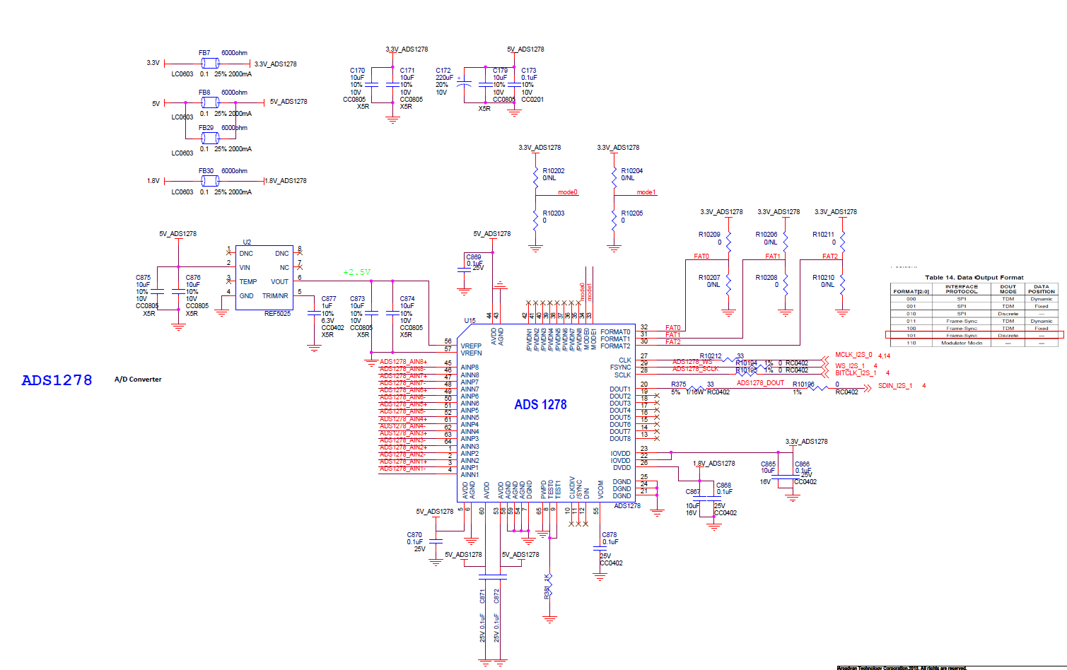
1. Checked the ADS1278 pinout; everything is correct.
2. AGND and DGND pins should be connected to the same ground plane. If using split ground planes, then connect both pins to the analog ground.
3. The /PWDNx pins must be connected to DGND or IOVDD. If all channels are powered up, then connect /PWDNx to IOVDD.
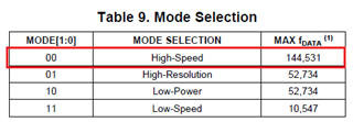
4. The Format pins are set to 0x101b, which uses all 8 DOUT lines. If you only want data on DOUT1, then use Frame-Sync TDM, 0x011b or 0x100b. Otherwise, all DOUTx pins must be connected to individual inputs on the host MCU.
5. DIN should be connected to DGND.
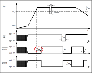
6. /SYNC must be driven. It is highly recommended to connect /SYNC to an IO pin on the host MCU. This pin functions as a reset, and is suggested to be pulsed after power-up and all supplies are within the recommended operating range. Please refer to the 'Power Supplies' section in the datasheet.
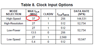
7. For Mode 00 (High-Speed), CLKDIV should be set to logic 1. Connect CLKDIV to IOVDD.
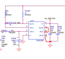
8. The SNR performance of the ADC has been tested using the REF5025 plus an OPA2350 buffer. The REF5025 can be directly connected to the reference input pins, but the SNR and THD may be degraded.
Regards, Keith Nicholas Precision ADC Applications
Thanks for your review. I have some question which need to inquire you.
1. Checked the ADS1278 pinout; everything is correct.
Edison :It' ok.
2. AGND and DGND pins should be connected to the same ground plane. If using split ground planes, then connect both pins to the analog ground.
Edison :I split ground planes , and connect them together . Please check.
3. The /PWDNx pins must be connected to DGND or IOVDD. If all channels are powered up, then connect /PWDNx to IOVDD.
Edison : I connect /PWDN1 to IOVDD , and other /PWDNx pins connect to DGND
4. The Format pins are set to 0x101b, which uses all 8 DOUT lines. If you only want data on DOUT1, then use Frame-Sync TDM, 0x011b or 0x100b. Otherwise, all DOUTx pins must be connected to individual inputs on the host MCU.
Edison :In our use case , we will use MCLK 22MHz or 24MHz. If we set 0x011b , does it support our design?
5. DIN should be connected to DGND.
Edison : It correct.
6. /SYNC must be driven. It is highly recommended to connect /SYNC to an IO pin on the host MCU. This pin functions as a reset, and is suggested to be pulsed after power-up and all supplies are within the recommended operating range. Please refer to the 'Power Supplies' section in the datasheet.
Edison : Add reset IC (EM6325CXSP5B-2.6). Please help check schematic.
7. For Mode 00 (High-Speed), CLKDIV should be set to logic 1. Connect CLKDIV to IOVDD.
Edison : I connect CLKDIV to IOVDD.
8. The SNR performance of the ADC has been tested using the REF5025 plus an OPA2350 buffer. The REF5025 can be directly connected to the reference input pins, but the SNR and THD may be degraded.
Edison :I add OPA2350 for SNR and THD performance. Please help check our schematic.
2. AGND and DGND pins on ADS1278 should be connected to the analog ground plane. Do not separate the pins using a resistor or ferrite bead inductor. The part will not work well and is more likely to be damaged from ESD or other electrical overvoltage transients. The original schematic for grounds is correct. Please make sure to connect both ground planes together and route the IOVDD and digital IO lines over this ground plane connection. You can refer to this E2E post for more details on proper layout and ground connections.
3. You have /PWDN1 connected to 3.3V and /PWDN2.../PWDN8 connected to ground. In this configuration, only channel 1 will be powered, all other channels, AIN2 through AIN8, will be shut down. Connect /PWDN2.../PWDN8 to 3.3V if you want to use 8 channels in the ADS1278.
4. Yes, mode 0x011b will send data for all channels on DOUT1, refer to Figure 79 in the datasheet for details.
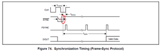
6. Power-on reset circuit will not work. After the supplies have stabilized and the ADS1278 asserts /DRDY (high to low transition), the /SYNC pin should be driven low for a minimum of 1 MCLK period, and then returned high for a full device reset. Please refer to Figure 74 in the datasheet.
8. The OPA2350 should work well. Do not leave pins 5 and 6 floating on the OPA2350. Connect Pin 6 to pin 7, and pin 5 to analog ground. Another option is to use OPA350.
4. You can use a clock of 22MHz or 24MHz for mode 00. This is O.K. For all modes using SPI, you can use any clock frequency in the range of 100kHz to 27MHz. For mode 00 and Frame Sync, you can use any clock frequency in the range of 100kHz to 37MHz.
6. Please give me a day to double check on the /SYNC pin requirement. We suggest a pulse, high->low and then low->high after the part has powered up. I am not certain how the part will respond if /SYNC is held low, and then transitions low->high after 200mS.
After further research regarding the /SYNC pin behavior, the power-on reset circuit should work well. In order for this to work, the power supply rails must be stable and within recommended operating voltage range. Also, the CLK signal must be stable to ensure a proper re-sync/reset.
Please make sure there is enough delay time for the power supplies and CLK to stabilize before the /SYNC pin transitions low->high.