Other Parts Discussed in Thread: ADS1120, ADS112C04
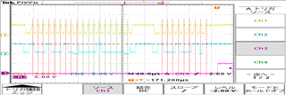
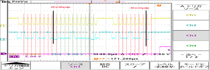
Yellow SCL
Blue SDA
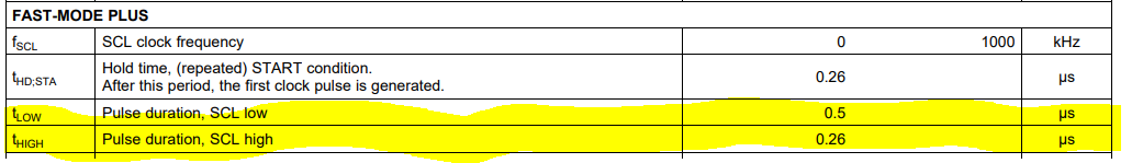
About the situation
Only the slave (ADS 1119 address is 0 × 49) and the master-side bus buffer (P 82 B 96 TD) are connected to the bus.
The following operations were performed when performing READDATA.
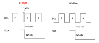
As indicated by the waveform of the oscilloscope, the slave IC returns ACK at 8CLK.
Question
・Why does the slave IC (ADS 1119) return ACK at 8CLK?
・Is there a solution?
Thank you and best regards,