This thread has been locked.

If you have a related question, please click the "Ask a related question" button in the top right corner. The newly created question will be automatically linked to this question.

DAC39J82: DAC39J82 and LMK04832 design review feedback

Part Number: DAC39J82
Other Parts Discussed in Thread: LMK04832,

7776.DAC_LMK_Schematic.pdf

Hi,

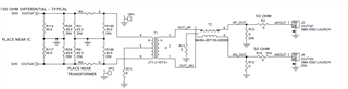
We have used 3 TI DACs of part number DAC39J82IAAV for Analog output generation. LMK04832NKDT is used for generation of JESD204B clocks and sampling clocks.
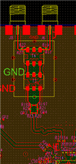
The schematic section has been attached, please provide review feedback for the design.

Design use details:

  1. All DACCLKP/N - AC coupled, LVPECL, 2520MHz
  2. All SYSREFP/N - Set as per lane rate and system clock frequencies, AC coupled option for DC coupling, LVPECL(AC coupled) LCPECL (DC coupled), <20MHz
  3. DAC WB,NB analog out (U31) - OUTAP/N: 407.5 ± 30 MHz, IOUTDP/N: 70MHz ± 2.5 MHz,
  4. DAC LO 1 analog out (U32) - OUTAP/N: 223.5 - 311.4 MHz
  5. DAC 3 analog out (U53) - OUTAP/N: 405 ± 37.5 MHz
  6. LMK Clock In 1 - 360MHz
  • Arunkumar,

    Sheet 23:

    1. Send the schematic to the high speed clocking forum so they can review the LMK04832 circuit.
    2. Not sure about the termination used for the CLKOUT0.
    3. May want to use the single-ended input clock circuit shown in Figure 24 of the data sheet to reduce part count.

    Sheet 25:

    1. Suggest adding a test point to SYNC_N_AB to allow you monitor the JESD SYNC signal status. Comes in handing when trouble-shooting the link during initial bring up.
    2. Add test points for ATEST and AMUX0,1.
    3. Add test points to the JTAG pins. This would allow you to perform Eyescan, read pattern verification errors and do real time monitoring of internal voltages and currents.  This would require connecting these signals to a PC running the IEEE 1500 instruction set. See data sheet for more details regarding this.
    4. CHD will be 180 degrees out of phase with respect to CHA due to the routing chosen. The outputs can be inverted in software to correct for this if needed.

    Sheet 26:

    1. Suggest removing R16, R17, and R18 to allow for thicker power plane routing. Using the resistors will force you to choke the plane routing. Do this for sheets 28 and 30.

    Everything else looks fine. Does the design use LDO’s or switchers for the DAC power?   

    Regards,

    Jim

  • Hi Jim,

    Thanks for your valuable suggestion.

    We have used LDO's for generation of  3.3 Volts, 1.8 Volts and 1 Volts  (Please refer to the  above attached Schematic). Also a 1V output Switching regulator for supplying to VDDDIG09  pins.

    Switching regulator specs:

    Switching frequency: 500Khz

    Peak to Peak ripple Voltage : 2.39mV 

    Regards,

    Arun

  • Please find the attached schematic in which DAC RX pins are interfaced with PL_MGT_JESD204B.pdfGTH Banks of Xilinx UltraScale Plus, MPSoC.

  • There was no power supplies shown in any of the schematics you sent.

  • Hi Jim,

    I have not shared as we have Used Analog devices Power Supplies to power DAC. Do you still want to have a look?

  • Arunkumar,

    No thanks. I think what you mentioned should be fine. The connections to the FPGA look fine as long the quads being used by an individual DAC can share the same reference clock per the Xilinx data sheet. 

    Regards,

    Jim

  • Hi Jim,

    Thank you for the response.

    In the below snip from DAC EVAL board

    Mini Circuit Transformer: JTX-2-10TA+, Ref Des: T1
    1. What is the significance of 75 ohm mentioned in the datasheet? (In our design we have used 50 Ohm)
    2. How that 75 ohm has effect on the impedance transformation in the above circuit across pin 1 & 3 with respect to the load impedance of 50 ohm?
    3. Is there any advantage in placing the RF line transformer(T2) between the DAC and T1 instead of between T1 and SMA connector?
  • Arunkumar,

    The impedance of the balun or transformer is not so critical, you can always re-match the impedance as needed for the circuit to work appropriately.

    The second balun/transformer is used to help balance the phase of the first balun/transformer in order to perserve the even order distortion at higher frequencies. The balun is also used to minimize common mode currents. I do not think this can be accomplished if you swap the order of the two parts.

    Depending on your application, the balun may not even be needed. 

    Regards,

    Jim

  • Hi Jim,

    The skew between the differential pairs of JESD204B sub 1 lanes can be handled it seems, so length matching not required is what told in the guidelines. How the upper limit of the skew is determined? Can you point to a document where it would be explained ? 

    Thank You,

    Arunkumar P

  • Arunkumar,

    The lane to lane skew is fairly tolerant for serdes interfaces.  The JESD204B spec calls out 3*SU (skew units) where a skew unit is the “max(UI, 320psec)” and only 1*SU is allocated to the PCB.  Here a UI is a unit interval of the serialized bit.  For 12.5GB/s operation the UI=80psec, so the skew would be limited by the 320psec constraint.  For a FR-4 PCB with the propagation delay is about 160psec/inch, so 20mils would only be 3psec. 

     The RBD value used by the DAC controls the amount of elastic buffer used. The larger the number, the more data that can be buffered to absorb skew, but the longer the latency will be. If this value is set to low, the buffering may not be enough to absorb the lane to lane skew.  

     Max value of K = 32. Max value of RBD is K-1 = 31. See attached file for more info regarding how skew can be absorbed by this buffer. See table 105 of the data sheet for RBD info.

    Regards,

    Jim

    1805.Achieving Deterministic Latency in a JESD204B Link.pptx

  • Jim,

    Is it possible to share the board file of EVM ? (.brd , allegro format)

  • Arunkumar,

    You can download the design files from the link below.

    Regards,

    Jim

    tidrive.ext.ti.com/.../7f6becef-0861-4ff0-af40-c5be7a3b7743

  • Hi,

    Can you please share the PCB actual stack up used ?

    It is to understand the trace impedance routing from DAC out to the SMA connector by estimating the trace widths. The stack up in the layout file is not correlating with the trace widths used.

    Thanks,

    Arunkumar P

  • Arunkumar,

    The file is attached. The complete design can be downloaded from the DAC39J82EVM product folder on the TI website.

    Regards,

    Jim


    DAC3XJ8XEVM-LYR_D.pdf

  • Hi,

    The stack up in the pdf or layout is mentioned that it is only for reference. If I use the stack up in stack up editor and compare the EVM board trace widths, impedance are not matching. If possible please share the stack up file that was given to manufacturing job, that would be the proper one.

    What is the routing strategy used for the layout in the above snip?

    The trace width just before and after balun are 19 mils and remaining till the DAC output are 9 mils. Is it like 100 ohm differential to 50 Ohm single ended transition? 

    Thanks

  • Arunkumar,

    See attached for vendor stackup used on this board. For your other question, the 19 mil traces are loosely coupled at 50 Ohms single-ended and the 9 mil traces are 100 Ohm differential coupled traces.

    Regards,

    Jim


    DAC3XJ8XEVM-FAB_D.zip