This thread has been locked.

If you have a related question, please click the "Ask a related question" button in the top right corner. The newly created question will be automatically linked to this question.

ADS127L11: Interface with FPGA

Part Number: ADS127L11
Other Parts Discussed in Thread: ADS8881

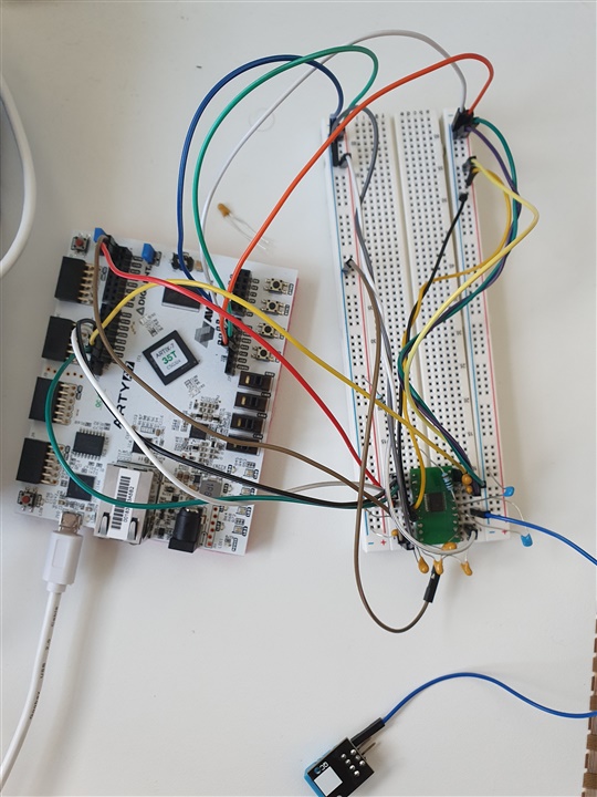
I recently bought this ADC and I want to connect its output (conversion result) to the FPGA.

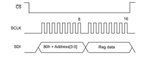
  1. How do I use it like a very simple ADC (analog in digital out), no registers, no programming etc. should i just feed the SDI pin invalid commands from the Master ?
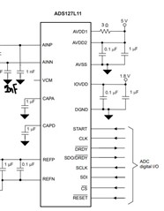
  2. Do I need to connect every pin to something ?
  3. If my analog input is single ended, do I just connect the negative analog input with GND?
  4. Can I use any power supply configuration for what I wanted in (1.) ?
  5. Do I have to connect bypass capacitors ?
  • 1. You'll almost certainly require some minimal programming of the ADS127L11 registers.  The output data rate and other basic settings are very unlikely to be correct for your application on reset.  The serial interface is well explained in the datasheet.  The NOOP command is useful when reading data

    2. Most pins will require a connection.  Section 9.2 shows a good example of a basic system.

    3. Probably.  Depends on your power supply configuration, but GND is a likely candidate.

    4. You can use any power supply configurations you wish that A) meet datasheet requirements, and B) support the measurement of the signals of interest.

    5. If you want any kind of performance whatsoever.  Without bypass caps and well thought out input filters, you may as well use a MUCH lower bit-count ADC as you'll never see anything close to 24 useful bits.

  • 1. I just want to read out the conversion results , thats all what I want from the ADC do i still have to feed commands to the SDI pin ? 

    Other Questions:

    1. How do I convert the output to fixed point ?
    2. Can I use another SPI mode instead of the prescribed one ?
  • Hello Youssef,

    The ADS127L11 has many options and requires an external clock for datasheet performance.  On reset, it defaults to an internal oscillator, and an internal register must be updated to enable the external clock source.  However, if you just want the device functional, you can connect SDI to ground, which will be interpreted as a NOP command, and the device will operate with the internal oscillator with an output data rate of about 400ksps.

    If you would like a simple, higher data rate device, then the ADS8881 is a 1MSPS 18b device that does not require configuration and may be a better fit.

    1.  The output of the ADS127L11 is a two's complement integer, which is already fixed point.

    2.  ADS127L11 only supports SPI mode 1.  At the hardware level, you can connect it in 3-wire or 4-wire configurations.

    Per Benjamin, you will need to use bypass capacitors; I doubt you can get the ADC to function without these due to noise generated on the IO lines.  Please refer to the ADS127L11EVM-PDK User's Guide for an example configuration schematic.

    Regards,
    Keith Nicholas
    Precision ADC Applications

    1. I'm sorry i'm a little bit confused, if i don't program the device (SDI to GND), do i get to read the conversion result from the ADC or not ? (when also providing an external clock ), or what do you mean by "just functional" ?
    2. if my analog input is single ended can i gnd the negative input ? 
    3. what should the ref-voltage be ? do i get to also connect both ?
    4.  so in total i need 6 bypass capacitor (CAPA;CAPB and 2 for AVDD; 2 for IOVDD) ?

    thanks for your and benjamin's answer Slight smile

  • 1. You'll read data so long as the START pin is high, but the device registers will be configured per reset specifications - which may or may not be ideal for your application.

    2. You can, as long as that's an appropriate place - we can't tell you if it is or isn't because we don't know what it's referenced to.

    3. It should be any voltage that meets the datasheet specification.  0.5V -> 2.75V for low range measurements or 1V -> (AVVD1 -AVSS) for high range measurements.  You need to connect something to both REFN and REFP as it's a differential input.  If your reference source is single ended, REFN could be connected to AGND.

    4. You'll need AT MINIMUM caps on AVDD, IOVDD, CAPA, CAPD, and some RC filtering on your input signal and reference voltage.  In order to even approach datasheet specifications for accuracy and noise, you'll need to consider all of these carefully.

    Have you actually read the datasheet?  Your questions aren't exactly hidden away in obscure places.

  • I had skimmed it when I asked these questions but then I began to actually read it.

    1. I am currently at the Register Descriptions part. But I have another question, I didn't quite understand when I write data to the registers (commands) , do I have to write them every frame or once at power-up and its stored in the registers forever unless I reset them?
    2. In order to write something I'd have to input (through the SDI) 80h+Reg_Addr. is this an addition or concatenation for example if i want to write something to register addr: 8h how would that look like ?
  • Hi Youssef,

    1.  The internal registers hold the last value that you write to them, so you only need to write them once after power-up or reset.  After the initial write, you can of course write to these registers again if you want to change the configuration of the device to something different.

    2.  In order to write to an internal register, you need to send a 16 bit word.  The first 4 bits are the write command, 0x8h, followed by the 4b address, and then finally the 8b data that you want to write to the register.  For example, in order to select the external clock, you would send the following 16b:

    0x8880h, or 0x1000 1000 1000 0000b

    As another example, if you want to enable the internal input buffers, you would write the following to the CONFIG1 register:

    0x8503h, or 0x1000 0101 0000 0011b

    Regards,
    Keith

  • Hi Keith,

    first of all thanks for your answer.

    After I configure the registers , should I then send in NOP to the SDI to read the conversion data in the following frame ? (I didn't quite get that part from the datasheet)

    Regards,

    Youssef

  • Hi Youssef,

    Yes, after configuring the register, you can just send a NOP (hold SDI low) to retrieve data.  Please take a look at section 8.5.6 in the datasheet for more details.

    Regards,
    Keith

  • Hi Keith,

    Okay thanks Slight smile

  • Ok now that I interfaced it with the FPGA. even though the analog inputs (signals to convert) are not even plugged it sends out data without me telling it to read a specific register. Do you have an idea what the issue is ?

    (I configured it by only writing to the config4 register that I want to use an external clock (20MHz) . After i press the button to write this command it sends this

    to the fpga) and nothing else but this. this waveform changes only when I want to read the config4 register (by pressing another button).

    Am i stuck at reading a specific register for example or what ? i really dont know why its only this waveform.  

  • The converter doesn't ever send out data on it's own.  It only responds on it's SDO pin when it's CS# is pulled low and SCLK is toggled.

    If you're sending NOOP (0x00) on the converters SDI pin, it is responding with converted data (Section 8.5.6 of the datasheet describes the behavior).

    The ADC has no idea whether anything is "plugged" in to it's input terminals.  It's converting whatever is there, even if that's just floating signals.

  • Hello Youssef,

    In addition to the device only responding when /CS is pulled low, the ADS127L11 is typically used with the START pin held high.  In this mode, it continuously converts data and updates the /DRDY pin by pulling it low when new data is ready to be retrieved.

    In this case, the FPGA needs to monitor the /DRDY pin and when it transitions low, you would then pull /CS low and clock out the conversion results.  This assumes that the SDI pin is held low; if the previous SPI frame issued a read register command, then you would retrieve the contents of the register.  These details are shown in Figure 8-27 in the datasheet.

    Hope this helps.  Have a nice weekend.

    Regards,
    Keith

  • Hi Benjamin,

    Yeah I know it wont ever send data on its own that's why I was wondering why there is the same output every frame, even if I didn't connect any analog signal to the analog inputs of the ADC. so I thought I was stuck at reading a register or something like that but I wasn't,  because after I configured the registers I sent NOP to the SDI Pin, so it should be reading conversion data.

    Then I found out that I wrongfully connected the reset pin (which is active low) to GND. Welcome to my life Slight smile

  • Hey Keith,

    Yeah I did that when I am in reading state I wait for the DRDY to go low and then pull CS low, but DRDY wont go low I don't know why. (I am using the default start/stop mode should I change it or something ?)

    Thanks for your help. You too. Stay safe.

    Regards,

    Youssef 

  • If you have the device configured for Start/Stop mode, and you have the START pin set HIGH, DRDY# should pulse LOW everytime a new conversion is available.  It's pretty difficult to break that functionality.

    If DRDY# isn't going low, then I'll bet one of the following things

    1) You've still got a problem with the RESET# pin.

    2) You don't have START set HIGH (or didn't issue a START command if you're not using the START pin for control)

    3) You've got DRDY# tied to something that is preventing it from going low.

    Posting your schematic would probably help.

  • 1) I tied the RESET# to IOVDD

    2) It is set High (sending a logic "1" from the FPGA)

    3) What can be preventing it from going low if I am passing the DRDY# to the FPGA through a GPIO pin on the board, and when in reading mode I wait for it to transition low, to pull SS# low.

  • 1) That should be good

    2) Have you verified this on board using a meter or scope?

    3) Are you sure it's connected properly?  Are you sure your FPGA pin is set as an input and isn't driving against the DRDY# signal?

  • 2) Do you think I should connect it with IOVDD too ? (I verified that it is sending out a logical '1' from the logic analyzer)

    3) Yes I am sure it is an input.

  • 1) There's no reason to do that as long as you're sure it's being driven high by the fpga.

    Why don't you tell us exactly what's connected to each and every pin on the ADC.  This part is so dead simple that you really shouldn't be having problems getting conversions out of it.  Getting quality conversions is a whole different issue, but getting DRDY# signals and data is blindingly simple

    If your DRDY# isn't toggling low, then something isn't hooked up right.

    Are you able to read and write registers? Does reading register 0x0C return 0x40, for instance?

  • Yes I am able to read and write registers. I configured the 4 registers and read what's in register config4 (and it was correct).

    Ok, I am using the same as this but /RESET tied to iovdd.

    • REFP<=3,3V
    • REFN<=GND
    • AINP<= Arduino Sound Sensor Analog output (KY-037)
    • AINN<= GND
    • AVSS<=GND
    • AVDD1<=5V
    • AVDD2<=5V
    • IOVDD<=3,3V

    The rest to FPGA 

  • My register setup is the following:

    CONFIG1: High ref range, and I am using the input buffers (REG_DATA<=4B)

    CONFIG2: extended input range (REG_DATA<=60)

    CONFIG3: sinc3 & OSR 26667 (REG_DATA<=1C)

    CONFIG4: external clock enabled (REG_DATA<=80)

  • And you've got caps on CAPA and CAPD?  You don't mention it, but I assume DGND is connected to GND?

    CONFIG2 = 0x60 makes no sense.  Bit 6 is reserved.  I'm guessing you want that to be 0x80.

    What happens if you set CONFIG4 = 0x00 to use Internal clock?  Perhaps your clock isn't working correctly.

  • Yes I have capacitors on CAPA and CAPD and DGND is connected. 

    Yes you are right I had it set to 0x80 but. It was a typo in my reply.

    I tried that also but it still the same problem occurs. I set the external clock to 25.6MHz (as per datasheet) and SCLK to 35MHz (it was written in the datasheet that minimum period of sclk was 20ns and max 1/4*(fdata) for IOVDD between 2V and 5.5V (section 6.8)

  • Hello Youssef,

    Checking the clock was my next suggestion.  Once the part is configured for external clock, it will not convert unless there is a proper external clock signal applied to the CLK pin.  This should be between 0.5MHz and 26.2MHz.  The /DRDY pin should be pulsing low at the output data rate with or without SPI communications at this point.  If it is not, then one of the pins is connected wrong, or the device is possibly damaged.  

    Can you provide a screenshot of your schematic showing all connections to the ADS127L11 pins?  If you are using the QFN version, then the power-pad should be connected to ground.

    Regards,
    Keith

  • I also monitored the CLK with Vivado's Logic Analyzer and it's working fine.

    All the connections to the pins are above in a reply message to Benjamin, or do you mean a photo of my whole setup ? if that's what you mean it's a little bit messy because I am connecting the pins through jumper cables.

    How can I verify that the device is not damaged ? (I am sending and receiving register data correctly)

  • Hello Youssef,

    Measure the clock frequency at the IC pin to make sure it is actually connected to the clock source.  Since your IOVDD=3.3V, the clock amplitude should also be 3.3V.

    I suggest using a DMM and measure all of the voltages at each of the pins to verify they are correctly connected to 3.3V, 5V, or ground.

    Without any communications, /CS=3.3V, START=3.3V, /RESET=3.3V, SDI=0V, you should be able to see the /DRDY pin pulsing at the output data rate.  Assuming you did not write to any additional register bits other than the CLK Select bit, then with CLK=25.6MHz, /DRDY should have a frequency of 400kHz.

    Regards,
    Keith

  • Hey Keith,

    Ok I will do that and I will get back to you with the results, but what if everything is correct and /DRDY still wont go low ?

    Regards,

    Youssef

  • If /DRDY won't go low, then either part is damaged, or connection is incorrect.  Those are the options.

    Simply powering it up in the configuration that Keith described will cause it to begin toggling DRDY.

  • Ok, thanks you so much for your help Slight smile

  • Hi Keith,

    So I did what you asked me to do, sorry it took so long.

    Like I said I am using it on a breadboard so everything measured was from the breadboard holes and from the I/O pins of the FPGA.

    The voltages are correct and the frequency of the clk also.

    /DRDY was also 3.3V but had a frequency of 8-9 kHz. What could be the problem ?

    Regards ,

    Youssef  

  • It should pulse at the Data Rate of whatever filter you've selected.  If it's pulsing though, then you're getting data - go read it.

  • I thought of that too but I am not getting any data out (conversion data) it's all zeroes

    But when I want to read a register it sends out the reg_data correctly.

    Besides, like Keith said, if I'm following his setup, which I did, it should pulse at 400kHz.

  • Can you take another Vivado Logic analyzer screenshot?  Please include the DRDY# signal.

    If you've programmed the registers for Sinc3-OSR26667, DRDY# should be pulsing at 480Hz.

  • Hi Youssef,

    You mentioned you are using a breadboard.  In order for the ADC to operate properly and reset properly on power-up, the bypass capacitors must be mounted directly next to the ADC and should be ceramic surface mount capacitors to reduce inductance.

    Are these capacitors mounted on the same PCB as the ADC and directly next to it?  I think a picture of your setup with your phone may be helpful.

    Regards,
    Keith

  • This is the setup.

    No the caps are not on the same pcb, but they are directly next to it. They are ceramic caps 

    And in reply to benjamin, DRDY was still the same as the pic above of Vivado's logic analyzer

  • Whoa.  I'm really trying to be gentle here, but that setup is horribly suspect.
    This is a 24 bit ADC with significant signal-integrity and power supply requirements.

    I see about 20 places where a short could have destroyed the analog section of the ADC.
    Literally none of the layout requirements are met.
    Not only are the caps much too far from the device, but they're connected using extremely long leads, which is really bad.

    I'm sorry to be the bearer of bad news, but without a much better setup, it's anyone's guess why it isn't working for you.

    There's a reason the EVM for this part looks like this ( even if TI did forget R94 and have to add it later :) )
    ADS127L11_EVM

    I really suggest buying one of the very reasonably priced EVM modules and hooking it up to your FPGA board.  The ADC works beautifully if it's powered and connected correctly.  I'm finishing up a design based on it right now, and I'm nothing but impressed with it's performance.

    ADS127L11EVM-PDK Evaluation board | TI.com

  • Hi Youssef,

    Ben is correct.  The through-hole capacitors in the picture of your setup will not work due to inductance of the long leads.  At a minimum, you need to have surface mount SMT capacitors placed directly on your adapter board directly next to the ADS127L11.  Highlighted below are the minimum caps needed.

    If you want to work with this device, the quickest way to start is to use the evaluation board.  Otherwise, you are going to need to solder all of these small parts directly next to the ADC in order to get it to operate.  In order to get anything near the data sheet performance, you will need a full custom PCB design.

    Regards,
    Keith