This thread has been locked.

If you have a related question, please click the "Ask a related question" button in the top right corner. The newly created question will be automatically linked to this question.

ADS124S08: Trouble Reading Valid Conversion Data

Part Number: ADS124S08

Hello,

This is a follow up question to:

https://e2e.ti.com/support/data-converters-group/data-converters/f/data-converters-forum/1022706/ads124s08-trouble-reading-conversion-data-with-internal-or-external-reference?tisearch=e2e-sitesearch

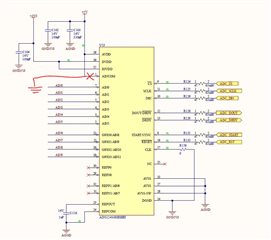
Since posting the previous thread, I determined that I had a bug in my software preventing the Reference Control Register to be written. Since then I have fixed this bug but am still not able to read valid conversion data. I am running the ADC with the internal reference, differential inputs (Ain2 tied to ground and set as the negative input, Ain9 set as the positive inputs signal and tied to a GPIO signal off the ADC). I have the PGA disabled and the internal reference buffers disabled.

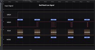
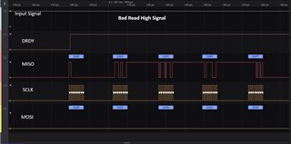
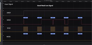
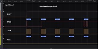
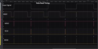
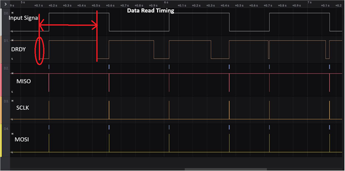
I have a ADC GPIO configured as an output which I have tied to the Ain9 input signal and I toggle it on every conversion reading. Although I would expect to read 0V and 3.3V conversion data based on this GPIO input, I continuously get conversion results that do not match what I expect. Occasionally, I will get results that look like they may be correct but that could just be a coincidence. I am using the slowest data rate of 2.5 SPS for debugging and am polling the DRDY pin for read timing.

Here are some screen shots of my coms:

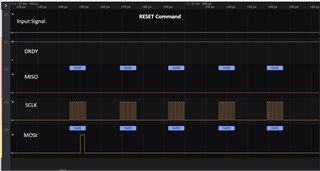
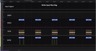
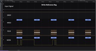
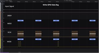
Initialization (There is a 3.7 ms delay between all initialization commands):

  1. Reset Command
  2. Configure System Reg 
    1. Enable Send Status
    2. Enable CRC
  3. Configure Input Mux Reg
    1. Ain2 = negative input 
    2. Ain9 = positive input
  4. Configure Reference Reg
    1. Internal reference always on
    2. Use internal 2.5V reference
    3. Disable both reference buffers
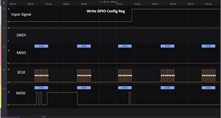
  5. Configure GPIO Data Reg
    1. GPIO 1 = Output
    2. Set GPIO 1 = high
  6. Configure GPIO Config Reg
    1. Set Ain7 as GPIO (GPIO-1)
  7. Configure Data Rate Reg
    1. Set to 2.5 SPS
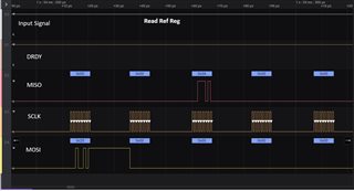
  8. Read back Reference Reg for debug
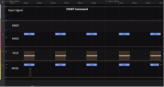
  9. Start Command

Reading Conversion Data:

  1. Bad low signal reading in through Ain9: Conversion results = 1,550,847
  2. Bad high signal reading in through Ain9: Conversion results = 6,946,233
  3. Good low signal reading through Ain9? Conversion results = 124,865 
  4. Good high signal reading though Ain9? Conversion results = 8,388,607
  5. Overall conversion reads showing timing
  • Hi Braden,

    It may be more helpful for me to see the actual Saleae plot, so if you can attach the file to the post I can then review it.

    When you toggle the GPIO you must make sure that the conversion restarts.  The conversion restart only automatically happens on certain register writes, such as changing the mux.  If you change the GPIO what happens is you will get a mix of sampling of both the high and low periods.  I think you may see better results if you send the STOP and START commands following the GPIO change.  The STOP command stops the ongoing conversion and START will restart the conversion.  START all by itself does nothing.  To restart conversions you must send the STOP command first followed by the START command.

    Best regards,

    Bob B

  • Thanks Bob, 

    Here is my full plot attached. I will also see if adding in the start / stop or not using the GPIO for testing helps the issue. 

    Thanks,

    Braden 

  • Hi Braden,

    The file didn't attach.  Please try again.

    For clarity see the following:

    The start of the next conversion period follows DRDY.  The time between falling edges of DRDY is the conversion period.  Note that the input signal changes during the conversion period which is a mix of high and low periods.  The result will be an average of the input signal during the conversion cycle unless you restart the conversion following the change of state of the GPIO.

    Best regards,

    Bob B

  • I see, that makes sense. The website is not letting me upload the .sal file so I uploaded it as a csv. I will test these updates tomorrow morning. 

    Thanks again,

    Bradendigital.csv

  • Hi Bob,

    I now have the input connected to an external supply and am not toggling any GPIOs. I have varied the external supply from .5V - 1.5V but can see the ADC always reporting conversion data ~6382003 or ~1.9V. I have attached my logic traces (channel 0 - DRDY, channel 1 - MISO, channel 2 - CLK, channel 3 - MOSI).

    Here is a breakdown of my startup procedure (3.7ms of delay between each command):

    1. Send reset command
    2. Read status reg - RDY bit = 0
    3. Clear FL_POR flag in status reg
    4. Configure SYS reg to enable CRC and status
    5. Configure mux reg to enable Ain9 as positive input and Ain2 as negative input (tied to gnd)
    6. Configure reference reg to use internal reference and disable buffers
    7. Configure data rate reg to as slow as possible (2.5 Sps)
    8. Send start message

    I have also verified that I get 2.5V on the REFOUT pin. 

    0714.digital.csv

  • Hi Braden,

    The csv file is pretty difficult to use and I do not know specifically what I'm looking at in terms of input voltage.  Maybe going back to the screen shots is better at this point.  Why not try keeping things as simple as possible.  I would just look at conversion results and not include status and CRC until you know you have communication working as it should.

    When you sent your schematic in the previous post, label AIN9 did not directly correspond to the ADC AIN9.  Are you sure you are using the correct mux selection?  The external supply should also have the minus connection connected to AGND as well as AIN2 connected to AGND.  The PGA must be disabled and bypassed.  You should see the voltage changing if the source is connected properly.

    Best regards,

    Bob B

  • Hi Bob, 

    I am not really sure what else to try at this point. I have uploaded the schematic with the current configuration that shows Ain9 connected to an external supply, Ain2 connected to AGND and AGND connected to GND3V3. Test point 49 is tied to AGND and test point 48 is tied to the positive side of the external test supply. The test supply is grounded to AGND.

    Here is a PowerPoint with screen shots of my communication after removing the CRC and Status bytes (using the default configuration). I am running the external supply connected to Ain9 at 1V and getting a conversion reading close to ~1.9V (~6369198). Note that I am still reading 5 bytes from the ADC which is an artifact of my code reading the status and CRC bytes before (Don't think this is an issue, just see the conversion data start to repeat).

    ASC_TIB_BUG_V2.pptx

    Thanks for all your help,

    Braden

  • I have also tried stopping the conversion each time I see DRDY go low, reading the data then starting again but still got inaccurate results.

  • Hi Braden,

    Can you read back the entire register map after your initialization routine and provide the data to me? It would help to make sure the ADC is in the intended state, and that the correct values are actually being written to the ADC.

    Have you tried measuring the inputs with a DMM, just to be sure that the voltage at AIN9 is actually 1 V with respect to ground?

    In the other post you mentioned that the digital and analog grounds are tied together - how? Is this at one point in the system, or is this a full ground plane that just happens to have different net names associated to it?

    -Bryan

  • Hi Bryan,

    1. I have attached a power point with screen shots reading from every register after my initialization routine has run. 
    2. I have measured and can see 1V appear across Ain9 and Ain0. I have also measured Ain9 with respect to ground on another test point on the board and can still see 1V
    3. It is a full ground plane

    At this point, I might buy the evaluation board for the ADC and try connecting it to my PCB for further trouble shooting unless you have any other suggestions. 

    Thanks for the help,

    Full_Register_Map.pptx

    Braden 

  • Hi Braden,

    Just to clarify, your INPUX register settings have you reading from AINP = AIN9 and AINN = AIN2. However, what you have labeled "AIN9" on your schematic corresponds to AIN11 on the actual ADC. I just want to confirm there is no issue there with a simple naming swap.

    Have you tried selecting different channels and seeing if the results improve? In other words, is this issue related to the specific channels you are measuring, or is this a system-wide issue that might indicate another problem e.g. poor layout?

    -Bryan

  • Ahh, the incorrectly labeled ADC input seems to be the issue. I believe things are working correctly now and will start testing at higher speeds. Thanks for catching that!

  • Sounds good Braden, hopefully it was this simple.

    I will consider this closed then for now. If you have further issues, please start a new thread and we can support you there

    -Bryan