Other Parts Discussed in Thread: TLV9064, REF50
Hi,
We are using ADS8528 for our development. Regarding the same we have some queries regarding the interface and the functionality.
We are using ADS8528 in our development boards with following configuration,
- HW Mode
- All CONVST_x tied together
- External Vref
- Internal clock
- Data collection through SDO_A and SDI line using in Serial mode (SPI).
- Not in daisy chain mode. Separate chip select for each ADC
- Over all 3 ADC used
With respect to the above configuration following are the queries regarding the functionality of ADS8528,
1. When used in HW mode with all CONVST_x tied together BUSY/INT (bit 27) act in INT mode. In order to configure this do we need to configure the config register using SPI line in SW mode? Also to change the polarity of the INT (Bit C26)
2. Now as per point 1, we need to change HW/SW pin to Software mode. Now, since the ADC is in SW mode, what is the status of other pins on the ADC like RANGE/XCLK? Since in HW mode, RANGE is configured for 2xVREF = 5V bipolar input, but in SW mode this pin behaves as external XCLK signal. How is RANGE defined in this case during the time the ADC remains in the SW mode? Will it change according to CONFIG register and reinitialize when device goes back to HW mode after config register update is complete?
3. In page 16 of the datasheet, tXCLK is mentioned as 66.67ns and clock cycles per conversion is 19-20 cycles. So, the conversion time tCONV=1.33us. But in HW mode by default, the device uses the internal clock CCLK for conversion, for which tCCLK is not mentioned in the datasheet. Is it the same as tXCLK?
4. The absolute maximum analogue input range on ADS8528 are HVSS-0.3V to HVDD+0.3V. In page 9, the HVDD minimum recommended voltage is specified as 5V, but the electrical characteristics are defined at HVDD=15V and HVSS=-15V. Since in our design we are using HVDD=5V, HVSS=0V, what will be the performance degradation when HVDD is at this minimum recommended voltage? Even though TLV9064 rails have been changed to 5V, the ADC input will be restricted to at least 100 ADC count below upper rail. Will there be a performance impact in that case?
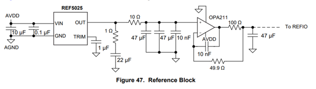
Also refer the updated attached schematic of all ADC and the reference (Vref) circuit, w.r.t above mentioned configuration and review the same and revert ASAP.
Best Regards,
Manish Sharma