Hi,
Regarding the DAC81416, is there any timing requirement between /LDAC and next data update cycle /CS ? The reason why ask is some channels of DAC81416 fail to output waveform as expected when we shorten the time between /LDAC and /CS.
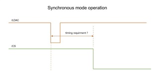
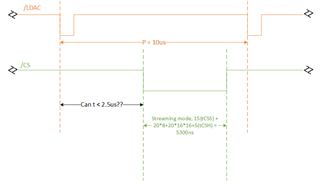
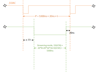
In our design, we use LDACs siganls of different DACs to synchronize output voltage on different channels, different DACs. We met the requirement tLOGDLY(cs rising edge to LDAC falling edge) described in datasheet, detail of our experiments as following:
1. At first, the LDAC rising edge to CS falling edge (a new round of data transmission) are: DAC0 150ns, DAC1 790ns, DAC2 1430ns. Then most channels of DAC0 won't work, only one or two could output correct waveform. DAC1 channel 2~15 could output correct waveform, ch 0 & 1 won't work (can only output a fixed voltage, guess the firstpoint of the waveform) . DAC 2 all good.
2.Then we delayed the transmission of DAC0 & 1 to 1430ns (LDAC rising edge to its own CS falling edge). All channels of all DACs are good.
3. Then we try to put DAC 0 & 1 earlier, but still meet the 1us wait time as described in chapter 9.3.1.2.1 of datasheet.
3.1 DAC0 1030ns (LDAC rising edge to its own CS falling edge), DAC1 1190ns. Then only ch1(2nd channel) of DAC0 won't work (guess only output first point of the waveform), other 15 channels of DAC0 all good. DAC 1 & 2 all good.
3.2 DAC0 later to 1140ns, DAC 1 1270. The same as 3.1, only ch1 of DAC0 won't work, rest all good.
3.3 DAC0 more later, 1190ns (the same as DAC1's time in 3.1), DAC 1 1300ns. The same, only ch1 of DAC0 won't work, rest all good.
BR/Wang Peng