Hi,
I attempt to control ADS7028 via TMS320C2000 Experiment Kit(Piccolo F28069).
After the last discussion
, Now I can read the ADC value correctly (I use a logic analyzer and a potentiometer to verify the function).
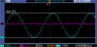
Now I want to enable the RMS and ZCD functions, input a sine wave (from waveform generator) into ch0, get its RMS value and output the ZCD waveform from ch7 at the same time, but neither function is working properly.
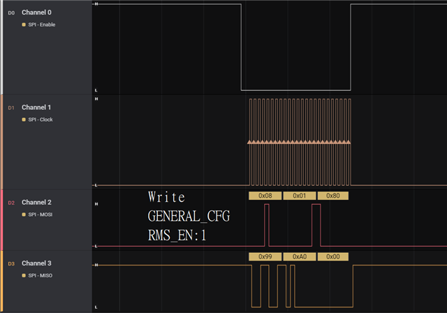
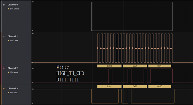
Ⅰ. In the RMS part
It seems that there are values stored in the registers, but when I adjust the amplitude of the sine wave and start the RMS process again, the value always remains the same until I turn off the power and restart.
The process is shown in the figures below:
1.Write RMS_CFG 1 time
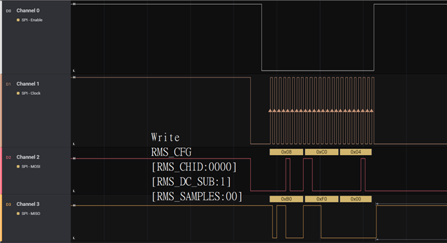
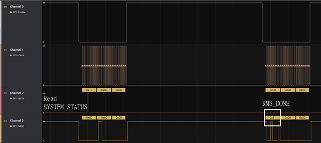
2.Start RMS computation
3.Poll the RMS_DONE bit in the SYSTEM_STATUS register
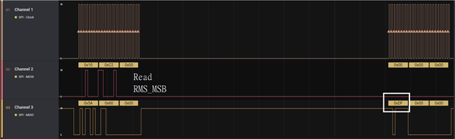
4.Read MSB
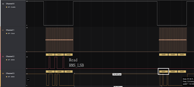
5.Read LSB
6.Repeat Step(2~5)
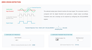
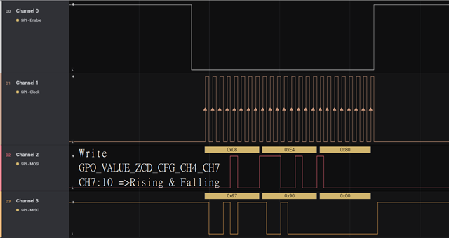
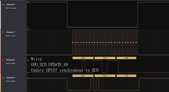
Ⅱ.In the ZCD part, my settings are as follows, but there is no output from ch7
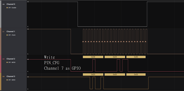
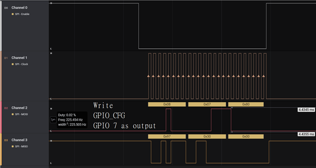
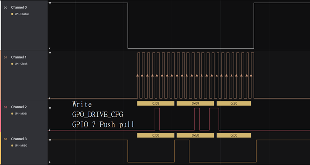
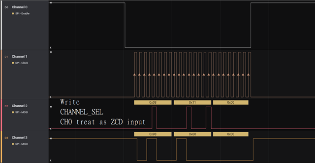
Please let me know if I missed any step or set registers incorrectly,thanks!