


1 Problem description:
Ø There are 24 registers inside DAC81416 Chip
Ø The address range 0x00 - 0x0e and 0x20-0x23 can be read and wirten normally
Ø The address range 0F~1F can be wirten(the output voltage of the channel is as expected),But All values read back are zero.

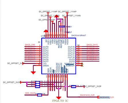
2 Chip Connect
Ø 3.3V power supply
Ø The pins SDO、SCLK、SDI、CS、CLR_n of the chip are connected to the FPGA.The FPGA use SPI protocol to control the chip
Ø TOGGLE0 TOGGLE1 TOGGLE2 connect to Ground
Ø CLR pin: the outputs of the FPGA is high
assign offest_clr_n = 1;
Ø RESET_n connect to 3.3V
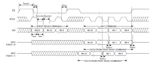
3 Write and read timming
Wirte and read in 24bit -mode,without CRC。
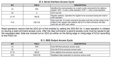
3.1 Write
Wirte access uses the 25MHz CLock
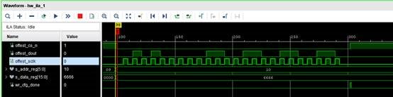
For example:The Address 0x10 is written as 0x6666
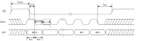
3.2 Read
Wirte access uses the 12.5MHz CLock
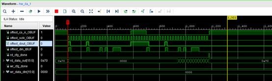
3.2.1 Read address 0x01 is correct(Device ID)
The address of the device id is 0x01,and the value is 0x0a70(as expected)

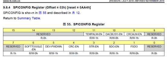
3.2.2 Read address 0x03 is correct(SPICONFIG)
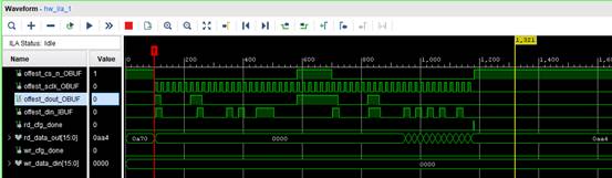
3.2.3 Read address 0x010 is no correct
DAC0 Register has been set to 0x6666,but the reset value 0x0000 is read

There are some other registers that have been configured
The register 0x003 has been set to 0x0a84
The register 0x004 has been set to 0x3f00
The register 0x005 has been set to 0x0000
The register 0x009 has been set to 0x0000


