This thread has been locked.

If you have a related question, please click the "Ask a related question" button in the top right corner. The newly created question will be automatically linked to this question.

ADS9234R: SCLK launch edge to next data valid on SDO delay

Part Number: ADS9234R

Hi,

The ADS9234R datasheet specifies the maximum delay time from SCLK launch edge to next data valid on SDO (td-ckdo 15.8ns for SDR). What is the minimum time delay? If we plan to read SDO pin immediately after SCLK launch edge how fast can we safety accomplish this?

  • Hi Erickson,

    After SCLK edge (falling or rising depending on SCLK polarity) has the td-CKDO to specify the maximum time before data on SDO is valid. It may be ready before but will take no longer than 15.8ns. I would suggest reading on the opposing edge of SCLK. So if data is output after the rising edge of SCLK, it would be ideal to read on the falling edge. 

    Regards,
    Aaron Estrada

  • Hi Aaron,

    Thanks for the reply. The datasheet also specifies the maximum Serial clock frequency (SCLK) with single data rate is 60MHz (16.7ns period). If our SCLK is 60MHz the data will not be ready until almost next clock cycle, missing the opposing edge of SCLK. Do these specs contradict each other or are we missing something?

  • HI Erickson,

    The td-CKDO spec is spec'd as a max time. So what it's saying is the longest possible time it will take for data to be valid after SCLK edge is 15.8ns. However, data may be ready before. So with a faster clock, I expect be ready sooner than the next edge. 

    Regards,
    Aaron

  • Aaron,

    The links below takes you to forum questions where the following is stated:

      --  td-CKDO does not depend on the SCLK clock freq. If SCLK = 60MHz or 1MHz, td-CKDO is still 15.8ns.

    Therefore, if I read SDO at the opposing edge of 60MHz SCLK there is a change I will not sample the latest SDO data. According to the guys in the other  forum I may be reading previous SDO data. What are you thoughts on this?  

    ADS7049-Q1: Delay time: SCLK falling to data valid on DOUT Max. 25ns. Is there a low limit? - Data converters forum - Data converters - TI E2E support forums

    ADS7029-Q1: Delay time: SCLK falling to (next) data valid on DOUT - Data converters forum - Data converters - TI E2E support forums

    Thanks
    Erickson

  • Hi Erickson,

    Thanks for providing some links to previous posts. The main support engineer is actually back in office sometime in the next few days so they will respond accordingly. I appreciate your patience on this!

    Regards,
    Aaron Estrada

  • Hi Aaron. That sounds good. When the main support engineer returns please ask him to help me address the following concern:

    In one of the links above Sandeep provided two workaround incase of faster SCLKs.
    1-  Implement a delay on the controller, as you mentioned.
    2- Treat the SPI as a full cycle interface - with data captured on the next fall edge of the SCLK.

    Lets say SCLK is 40Mhz and td-CKDO max is 15.8ns and the data is shifted out on the falling edge of the clock (SPI MODE 0). In this configuration sampling SDO on the rising edge of the SCLK will not work because SDO will be sampled 12.5ns after the shifting edge and fail td-CKDO requirement. If I use one of the workout provided by Sandeep, SDO can be sampled at the next falling edge which will be 25ns after the shifting edge. Will this work for this chip? Can we SAFELY do this?

    Knowing the minimum delay between SCLK falling edge and data valid on SDO (td-CKDO Min) will help us. Can it ever be 0ns? or is it 2ns, 6ns ,10ns?

  • Hello Erickson,

    Thank you for working with us on this post. Either of the techniques Sandeep outlined in his other thread can be applied to the ADS9234R as well. We cannot guarantee a minimum clock-to-data-valid spec since we do not characterize this delay. A more robust approach would be to consider the max t_CKDO spec and apply one of the workarounds above. 

    Remember that in SPI Mode 00, the CSn falling edge will shift out the MSB after tDEN_CSDO (max = 12 ns). Then you can begin sending SCLK, where the first SCLK falling edge will launch the MSB-1 bit while the host captures the MSB. You will need one extra clock period to read all the data, but this is ok since the frame ends with the CSn rising edge, which resets the interface and begins the next conversion cycle.

    Regards,

    Ryan

  • Hi Ryan,

    We will go with sample/capture on the same edge workaround. Thanks for clarifying.

    I'm trying to understand your last point before closing this forum discussion.

  • Hello Erickson,

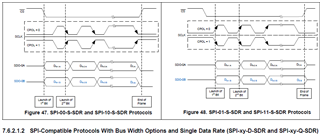
    I believe I need to retract what I said about needing an "extra clock period." Due to the inherent SPI propagation delays, you should be able to latch data on the same edge as the next bit is launched without issue. In SPI Mode 0, since the MSB is launched by the CSn falling edge, you do not need extra clock periods:

    • CSn goes low, launches MSB
    • 1st SCLK rising edge latches MSB (bit 15), launches MSB-1 (bit 14)
    • 15th rising edge latches LSB+1 (bit 1), launches LSB (bit 0)
    • 16th rising edge latches LSB (bit 0)
    • CSn returns high

    Let me know if you need any additional help with this.

    Regards,

    Ryan

  • Hi Ryan,

    I sketched several waveforms to make sense of this. I came to the same conclusion. Thanks for confirming.

    In SPI mode 0 data is launched on the falling edge. You stated:

    • 1st SCLK rising edge latches MSB (bit 15), launches MSB-1 (bit 14)

    But it should be:

    • 1st SCLK falling edge latches MSB (bit 15), launches MSB-1 (bit 14)

    Agreed?

    Erickson

  • Hi Erickson, 

    Yes, my mistake. In that case, the falling edge (or more precisely the "trailing edge") will launch all subsequent bits, while simultaneously latching the previous bit. Still 16 clocks in total.

    I've included Figure 7.6.1.2 below for others to refer to as well.

    Best regards,

    Ryan

  • Hi Ryan,

    Great! Thanks for the help.