This thread has been locked.
If you have a related question, please click the "Ask a related question" button in the top right corner. The newly created question will be automatically linked to this question.
We are implementing the ADS1293 in at least 100 devices these coming months, and we would like to confirm a few questions:
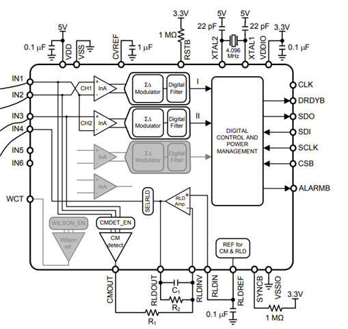
1) Does it need 3.3 V and 5 V as indicated on the schematic on page 63 of the datasheet, or can we simply use 3.3 V everywhere? What effect on performance will this have?
2) Does it need the external clock (XTAL 1 & 2)? In what cases does it need it? What effect on performance will it have?
3) We have attached a ground reference electrode (E_G) in our previous design with the ADS1292 at RLDREF which has worked well, is this the correct thing to do for the ADS1293?
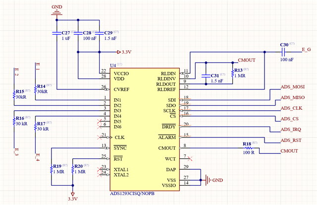
Other than these changes, my schematic follows the datasheet (both pictured below), can someone please comment if they think my design will work and suggestions?
Thank you in advance!
Hi Bryan,
Welcome to the E2E forum !!!
Please see my comments below for your inquiries.
1) You can use 3.3V for both VDD and VDDIO power supplies. Please refer to section 7.3 in the datasheet for the recommended operating conditions. Unless otherwise noted, the device's electrical characteristics are specified with the full power supply range. You can verify the specification for your operating requirements.
2) You will need a clock to operate the device. The clock can be either provided externally on the bidirectional CLK pin or with the on-chip crystal oscillator. The on-chip crystal oscillator will need an external 4.096 MHz crystal connected between XTAL1 and XTAL2 for operation. Please refer to the Clock Oscillation section for more detailed information on the clock configuration.
3) The flexible routing switch on the ADS1293 is different from the ADS1292. Please check the ADS1293 flexible routing switch configurations (section 8.3) to verify you are able to accomplish what you have done with the ADS1292.
Thanks
-TC
Hi TC, thank you for clearing up my questions, however in question 3, I don't think I was referring to a flexible routing switch. I was referring to the feature of right-leg drive, where E_G is an electrode which is compared with CMOUT according to 8.3.12. So, I think my schematic is correct then to attach the electrode at pins 11 and 12?
Hi Bryan,
Thanks for the clarification.
The internal RLD amplifier for the ADS1293 is very similar to the ADS1292. However, the RLDOUT output for the ADS1293 can be routed to the INx through the flexible routing switch or connected using the RLDOUT pin. Please refer to the diagram you attached (Figure 84) for how the RLDOUT is connected to the RL electrode.
Thanks
-TC