Other Parts Discussed in Thread: OPA171
Hi,
We are using two ADS8556 in serial interface (not in daisy chain). I have following questions on front end and circuit configuration:
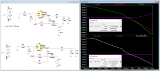
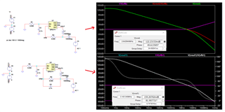
- For front end where signal frequency is up to 4.4KHz (including Harmonics), non-inverting configuration is used. From stability point of view, there are two circuits one with CF and without CF. The phase margin with both circuits is above 45 deg (for stable op PM >=45deg). However, with CF PM increased to 81.9deg. Do you recommend using CF as it will increase PM to 81.9deg? Please confirm. (Refer below image)
- Input signal to above circuit is the output of voltage/current sensors, does non-inverting configuration help in achieving high input impedance? Is it required?
- Generally non-inverting configuration is more prone to stability issues and CMRR of configuration is also not good.
- Is inverting configuration required here? as recommended in application circuit in datasheet.
- We have two ADCs (ADS8556), their BUSY signal is monitored using diode ORing. I saw in one of the posts which says it is not recommended and suggestion is to use OR gate? Can you explain why?
- For hardwire based configuration, what is the recommended values of pull up or pull down resistors?
- In datasheet 49.9 and 370pF is used on analog inputs which provides Fc = 8.6MHz and RC = 18ns. Datasheet further mentions that this RC will reject high frequency noise and meet settling requirements as well. What is the settling time requirement? It will help me to choose appropriate values for RC.
Regards,
Sunney