This thread has been locked.

If you have a related question, please click the "Ask a related question" button in the top right corner. The newly created question will be automatically linked to this question.

ADS5263: bitwise mode in ads5263

Part Number: ADS5263
Other Parts Discussed in Thread: ADS5294

hai,

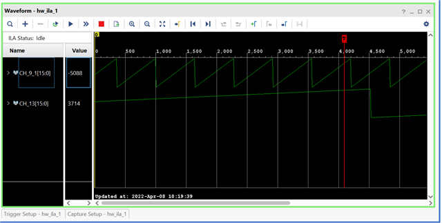
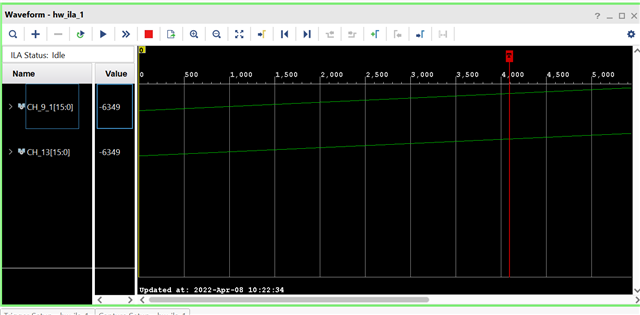
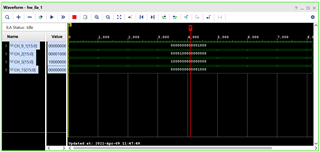
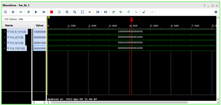
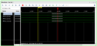
There's no mention in ads5263 data sheet regarding how to configure it as bitwise mode and in one of the posts as i read writing the 0x28 register with 0x8100 will make it bit wise does this work every time or is der any problem in this because im not getting output continuously, after writing the register twice sometimes more than that then I get output basically my output is not stable only if i write register more than once i get output  is there any problem when we write 8100 to 0x28, or is it something else please help me.   

  • Hi Mohith,

    I think the settings are correct 0x28 0x8100 and should enable the bit wise mode in ADS5263. 

    I am sure about the settings because in the other E2E post, Chen mentioned that we have tested the same and also I have looked similar other ADC datasheet as well for eg. ADS5294, there they have shared more details of this mode. 

    I think it may be a capture issue. As from other post, can you verify that:

    1.  Are you using the ADS5263 GUI.

    2. When you are using TSW1400 EVM to capture the output data from ADS5263, you also need to make sure you can load the correct ini file, in order to run High Speed Data Converter Pro GUI correctly.

    Thanks & regards,

    Abhishek

  • Hi Abhishek,

    Thank You for your reply,

    We are using custom board with ads5263 chip no not ads5263 gui, with xilinx zynq board and select i/o ip, please let me know if i have to take care of any corner scenarios either in hardware or firmware code so that there's no capture issues.

    I had one more observation if i generate ramp test pattern using the the register 0x25 with data 0x0040 im always able to see the ramp but every time i write this register no of samples of ramp changes i mean to say the ramps become larger sometimes small i have attached some ila output snips for your reference.

    With Regards

    Mohith RS

  • Hi Mohith,

    Thanks for sharing the waveforms and more information.

    From what I could gather so far is these problems usually are related to interface, or improper deserialization. Below points are specific to what you are observing:

    1. Ramp may become erratic when there is a bit slip or when deserialization is not happening properly. What I mean is say 1 bit is not at its right place after deserialization due to some bug (eg. after capture say the order somehow becomes D7...D0,D15, D14..D9, then every time D0 toggles you will see 2**8 code change instead of 1 code change). In order to verfiy/eliminate this possibility, you can -

      --- test with custom data pattern and keep only 1 bit high rest zero, then do the capture and see if you see the bit moving or shifting capture to capture - share us the observation.

    2. Another possibility could be related to FPGA configuration whenever you change the LVDS output mode. Usually, good practice is to reinitialize FPGA capture settings after doing output data mode change or serialization factor change etc.

    Let me know if the above helps or you get some indication as to where exactly the problem lies. 

    Also, just one more thing, is it happening on multiple devices or just this one? If you haven't checked on multiple devices/boards, I recommend you to please try the same on multiple device if possible.

    Thanks & regards,
    Abhishek 

  • Hi Abhishek,

    Thank you this discussion is really thought provoking, and really helpful.

    As you told I tried with custom pattern with these settings (0x25,0x0018) and (0x26,0x8000) bits are shifting every time I write the register, below are some snips of the output.

    Yeah, it is happening with all the chips, we've purchased 8 chips and it is happening in all the 8 chips.

    And yes every time  we write spi register to change output mode we're reinitializing the data capture settings.

    one more observation which I wanted to discuss is whenever I do global power down 0x0F,0x0200 either bits should be initialized to all 0s or either all 1s but sometimes it all 0s and sometimes its some bits will become one i will attach these snips too.

    If it is because of bit slips can you please tell me how to avoid it or help me with any solution.

    Thanking you With regards,

    Mohith RS

  • Hi Mohith,

    Thanks for sharing the information.

    I had discussed the same within my team as well on this.

    Since all the devices are showing this bit slipping, which indicates that the there is some issue with the FPGA  code implementation. Because the device does not change any bits on its own. 

    Also we have tested the bit-wise mode and we do not see any problem.

    We recommend you to:

    1. Check the data alignment in the FPGA with respect to the FCLK (data relationship with frame clock)

    2. Relook the FPGA code implementation in terms of data separation logic.

    Thanks & regards,

    Abhishek

  • Hi Abhishek,

    I tried with few changes in the RTL adc data capture, problem still persists will you be able to help me with the RTL, or any reference RTL if you can share it with me it will be really helpful, we're about to deliver the project if your suggestions will be of great help.

    Thanking You with Regards

    Mohith RS

  • Hi Mohith,

    Sorry to hear that. 

    As for the suggestion, you can probe the device output directly on the scope by programming the device in known test pattern. If output is looking expected then it has to be debugged in the FPGA only. 

    Unfortunately we don’t have any reference RTL code since the device was released quite a while ago somewhere around 2011.

    Thanks & regards,

    Abhishek