This thread has been locked.

If you have a related question, please click the "Ask a related question" button in the top right corner. The newly created question will be automatically linked to this question.

AFE5832LP: Came across problems using AFE5832LP and please help

Part Number: AFE5832LP
Other Parts Discussed in Thread: AFE5832,

Hi Sir/Madam,

when we use AFE5832LP device to develop portable ultrasound for medical application, we came across a problem as follows and do not know how to solve this. Since this is the 1st time using AFE5832,could you help us to solve this problem. Thank you very much!

Best regards,

Kevin Niu

AFE5832 Debug Questions.docx

//Register  0X01

//BIT 14 LVDS_RATE_2X  0 = 1X rate                      1 = 2X rate

//BIT 5  DIS_LVDS      0 = LVDS interface is enabled    1 = LVDS interface is disabled

//BIT 14 GLOBAL_PDN    0 = The ADC die operates in normal mode  1 = The ADC die enters complete power-down mode

AFE5832_CFG(0x01, 0x0000);


//Register  0X03

//BIT 15-13 SER_DATA_RATE   011 = 10X

//BIT 12    DIG_GAIN_EN     1 = Digital gain enabled

//Bit 4                     1,must

//0111 0000 0001 0000

AFE5832_CFG(0x03, 0x7010);


//Register  0X04

//BIT 8     PAT_SELECT_IND    0 = All LVDS output data lines have the same pattern

//BIT 4     MSB_FIRST         1 = The MSB is transmitted first on serialized output data

//Bit 3     DATA_FORMAT       0 = Twos complement format for output data

//Bit 1-0   ADC_RES           11 = 10-bit resolution

//0000 0000 0001 0011

AFE5832_CFG(0x04, 0x0013);


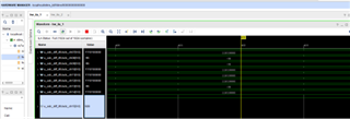
In DESKEW mode, the register 0x02 = 0x2100, in fpga system, the data 0101010101 captured by ILA capture is right.


In sync mode, the register 0x02 = 0x2080, in fpga system, the data 1111100000 captured by ILA capture is right.


In All 1s mode, the register 0x02 = 0x2200, in fpga system, the data 1111111111 captured by ILA capture is right. 


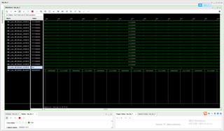
In RAMP mode, the register 0x02 = 0x2380, in fpga system, the data captured by ILA capture is error. 


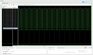
In RAMP mode, the register 0x02 = 0x23C0, in fpga system, the data captured by ILA capture is error too. 


  • Hi Qi Niu,

    Thanks for reaching out to us. In-order to understand the issue better I have couple of questions. Can you please answer them,

    Are you using Frame Clock to detect the frame boundary for all the LVDS_OUT lanes ?

    If yes, could explain why are you setting PAT_MODES_FCLK to '001' in all your test pattern settings? Setting this will change the FCLK behavior.

    If no, how are you detecting the start of frame for each LVDS lane in the FPGA.

    We tested the ramp pattern in 10bit and 12bit mode and it works as expected. It would also be helpful for us to know how the architecture of LVDS deserializer is implemented in your FPGA card. If you feel you like you can't share any specific information on public forum, you could also reach out to us via support_us_afe_tx@list.ti.com.

    Regards,
    Kalyan

  • Hi Kalyan,

    Thank you very much for you prompt reply and I have sent an email to support_us_afe_tx@list.ti.com regarding my specific problem.

    Thank you again!

    Best Regards,

    Qi

  • Hi Niu,

    Thanks for reaching on the support group. Kalyan will support you further over the mail.

    Regards,
    Abhishek

  • Hi Abhishek,

    Thank you for your information and I am looking forward to Kalyan's kind helps via email.

    Regards,

    Qi

  • Hi Kalyan,
     
    Thank you very much for your prompt replies and kind helps. We have found the reason and solved the problem. The problem is that  the voltage level we set was not satisfying the level which is  specified in the datasheet, as you suggested to us.
    Thank you so much for your so kind and valuable helps!
     
    Best Regards,
     
    Qi