This thread has been locked.

If you have a related question, please click the "Ask a related question" button in the top right corner. The newly created question will be automatically linked to this question.

ADS1282-SP: Device damaged when AVDD was absent while VREF was present.

Part Number: ADS1282-SP
Other Parts Discussed in Thread: ADS1282

Dear Christopher,

in order to keep the reference voltage as stable and clean as possible, I connected the AVDD pins to a dedicated 5V_SENS power supply sourced by a linear voltage regulator and kept the VREFP pin connected to a reference 5V generated by an AD584 reference generator with an external NPN transistor.

It happened that my 5V_SENSOR power supply was switched off because of a supposed failure, while VREFP stayed switched on.

The ADC started sinking 40mA on the AVDD and providing acquisitions with doubled value as it was selected PG = 2. All commands were perfectly interpreted and implemented by the ADC and, by the way, I continuously write CONFIG1 register to keep PG = 1 selected. Furthermore, I checked the output of the PGA and it was giving evidence of a 1x gain selection.

I deemed the ADC as damaged and removed it from the PCB.

My question is:

Could the presence of VREFP while AVDD was absent be the root cause of ADC failure?

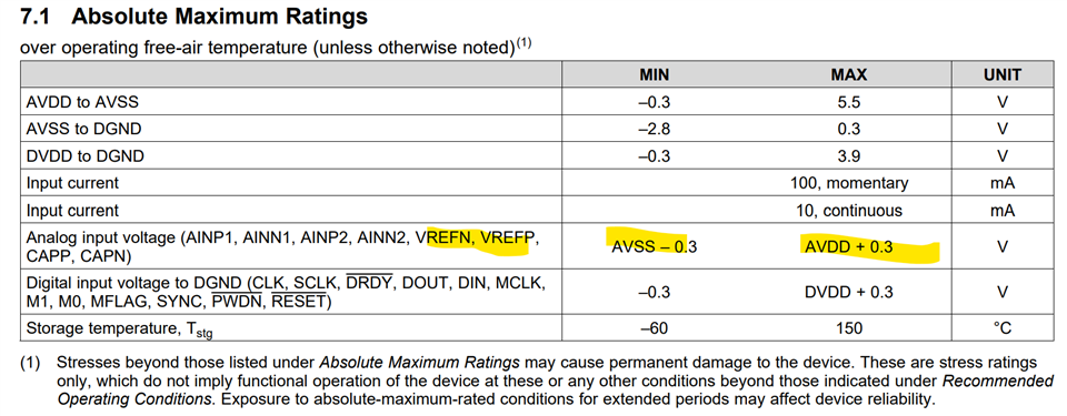
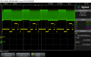
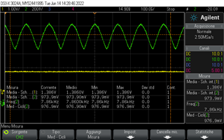
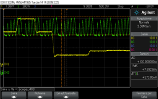
Additional information: the ADC, because of the absence of many sensors, resulted also fed by a 12V input for about 16ms in a 50ms period (1/3rd of the period) absorbing  about 11,5mA on AINP pin - (12V-0.6V)/1kohm -, which is more than the 10mA continuous input current limit but much less than the temporary 100mA input current limit.

Thanking you in advance,

Best regards,

Daniele Lippi

  • Hello Daniele,

    Unfortunately, yes, the presence of VREFP while AVDD was absent could absolutely be the root cause. In fact, it is a very likely root cause.

    As you can see from the absolute maximum ratings, the voltage on the VREFP pin should not have exceeded 0.3V if AVDD = 0V (or if was floating for that matter). When a device pulls more than the nominal operation (or quiescent) current than the datasheet spec, its a good inidication that the device is damaged. Especially if it persists through power cycling.

    Can you provide some more clarification on the additional info? Is the AINP input also exposed to 12V? I understand that there might be an input current between the two specs and I will talk with the team if there is a concern there. However, I couldn't understand if this behavior was periodic during your normal operation and not just during start up or during some other criteria. 

    Thanks,

    -Cole

  • Hi Cole,

    thanks for your prompt reply.

    Here below I'll give a clarification of the 12V AINP pin exposure.

    AINP is currently exposed to12V input for about 16-20ms over an acquisition repetition period of 50ms. That's a non nominal behaviour for my system, that is expected to have all sensors properly connected and providing inputs in the range AVSS+0.5V to AVDD-1.25V.

    Anyhow, my circuit provides a 1kohm resistor on that line to limit the current sunk by that pin through the protection diode. I'll increase that resistor to at least 1.5kohm in order to respect the continuous input current maximum rating of 10mA.

    When the damage occurred, the external MUX was selecting a close to 0V signal, so the input was at 1V, that is the offset I add to respect the AINP, AINN >= AVSS+0.5V constraint.

    DL

  • Hello DL,

    Thanks for the context. Unfortunately, whether the real system would be like this or not, 12V on the inputs still violates the absolute maximum ratings of the device and could damage it. You might want to consider some external protection such as a 5V Zener diode  (e.g. https://www.digikey.com/en/products/detail/nexperia-usa-inc/PLVA650A-215/1163688) on some of these inputs if you expect this behavior in future.

    Yeah, I expect the reference was the problem then. If you want to verify this, you can try and do an impedance test with something like a DMM between the VREFP and AVDD to AVSS or GND pins to see if there was a short circuit between those pins. I will note, its better to take the device off the PCB to remove any possibility of coupling elsewhere in the circuit, or you can compare against a known good PCB to understand if the system deviated from a nominal case.

    I also agree, increasing the current limiting resistor should help keep the device within the spec. I would expect some more error to be contributed from these larger resistors on the input.

    Best,

    -Cole

  • Hello Cole,

    in the meanwhile some modifications were implemented to increase the quality of the reference voltage: I separated AVDD from VREFP together with a system to ensure that VREFP is present only in case AVDD is present and also making the former being less than AVDD+0.3V (Schottky Diode between VREFP and AVDD) and an enbedded control in FPGA.
    As regards AINP, AINN protections, I implented the replacement of 1kohm series resistor with 1.5kohm resistors to limit the input current to <10mA.

    As a result, now I noted that AINN oscillates with a frequency of about 8kHz and the same happens on CAPN (input of the modulator). This oscillation (360mVpp/8kHz) is removed bypassing the AINN protection resistor. Also the acquisitions of my ground reference (this reference is input to a MUX and then filtered as well as offset by 1V; same offset on AINN) reflects this observation: in the first case I can read about 160mV; in the second case 534uV.

    Observing the attached oscilloscope screenshots, you can see that AINN (1V nominal) seems to be clamped at about 0.65-0.8V.

    Furthermore, I observe MFLAG signalling that modulator is generally overdriven. This is likely due to the fact that the oscillations on AINN cause modulator's overdrive. Unfortunately, also with AINN resistor bypass, MFLAG activates sometimes, even though I couldn't find any noticeable reason for that.

    Finally, I observed a 60mV voltage drop across the AINN protection resistance, pointing out an average 40uA current flowing into AINN pin , when I expected something like 1nA as specified in the datasheet.

    NB: all inputs were always within the acceptance range (AVSS+0,7V to AVDD-1,25V). No out of range input was ever provided to this device.

    Attachments:

    all figures below refer to the presence of 1k5ohm  rprotection resistors on both AINP and AINN.

    Legend: CH1 = AINP (yellow); CH2 = AINN (green)

    Figure 1 - AINN wrt AINP

    (during SINC acquisitions CM is lower and clamping seem to occur; during FIR acquisitions CM is higher and clamping seems not to occur)

    Figure 2 - AINN during FIR acquisition

    Figure 2

    Figure 3 - AINN during SINC only acquisitions

    Figure 1

    It could be damaged, but this time I don't find any actual reason for that, especially given all the precautions i took before using the ADC.

    What do you think?

  • Hi Daniele,

    Cole is on holiday this week.  He is back in the office on the 20th.  In the meantime, you shared a schematic snippet with Chris on your previous thread.  Is that schematic still valid with the exception of the 1k5 series resistor and the Schottky?  Can you tell me what is the difference between the CH1 input in Fig 1 and 3 versus Fig 2?

  • Hi Tom,

    the circuit has not changed except for the protection resistors value and for the use of 5V_SENS to feed AVDD and 5V_ANALOG to feed VREFP, keeping them linked by means of a Schottky diode with A on VREFP and K on AVDD, in order to avoid VREFP > AVDD+0.3V, Furthermore, 5V_ANALOG is limited to 9mA.

    Figure 1 shows the overall behaviour while Figure 2 and Figure 3 are details of the same waveforms in Figure 1.

    Figure 2 zooms the part where I'm performing FIR/4kSpS acquisitions (I get the first nDRDY negedge after SYNCing the ADC to void filters, thus AINP is fed by the same signal for 16ms + 250us Sallen-Key LPF settling time)

    Figure 3 zooms the part where I'm performing SINC/64kSpS acquisitions (I get the first nDRDY negedge after SYNCing the ADC to void filters, thus AINP is fed by the same signal for 450us + 250us Sallen-Key LPF settling time).

    The oscillations observed are all 8kHz.

    Regards,

    Daniele

  • Thank you for the clarification Daniele!

  • Hey Daniele,

    My bad on the "TI Thinks Resolved" I clicked that button instead of the Reply button.

    Anyways, I'm really confused what I'm looking at. From what I can tell AINN is oscillating and not expected by you. For AINP, it looks like a DC type voltage that can change to some piecewise waveform that is periodic and this is expected. Is this correct?

    MFLAG tripping is an interesting sign but expected given the waveforms. AINN = around 0.5mV, and AINP = 5V max, so we're violating every FSR option in the device. I'm trying to understand if AINP is expected and what AINN is supposed to be. Looking at the schematic in the post that was created from this one, it looks like voltage divider into a buffer that provides 1V_DC, but that would still exceed FSR if that was expected.

    What I would do as a debug step is removing the current limiting resistors on the inputs, so the inputs are isolated from the buffers, and then force a known voltage from a bench top supply (with a current limit between AINP and AINN) and read the output. That way we'd at least understand if the ADC is functioning as expected. 

    Best,

    -Cole

  • Hi Cole,

    AINN input scale is 200mV/div. Given that, AINN results an average of 950-1000mV with 350mV peak-to-peak voltage. MFLAG triggered active/inactive because many times the difference between AINP and AINN went slightly overrange and the root cause was AINN oscillation.

    Looking at the schematic in the post that was created from this one, it looks like voltage divider into a buffer that provides 1V_DC, but that would still exceed FSR if that was expected.

    1Vdc is generated and provided both to AINN and AINP to make the resulting waveform stay between 1V and 3.5V in order to prevent violations of the input limits (VSS+0.5V; VDD-1.25V), since the ADC AVDD is 5V and AVSS is 0V.

    It's true that Figure 3 points out a signal exceeding 3.5V, but it was the only one. The waveform is periodic because it is given by an external analog MUX sweeping 32 different inputs, that are all fixed dc.

    MFLAG was correctly activated, not only when the input was violating input limits, but whenever the input differential voltage was exceeding Vref/2. The latter violations were all due to AINN wide oscillations.

    What I would do as a debug step is removing the current limiting resistors on the inputs, so the inputs are isolated from the buffers, and then force a known voltage from a bench top supply (with a current limit between AINP and AINN) and read the output. That way we'd at least understand if the ADC is functioning as expected. 

    We've already done this test, by feeding the ADC with fixed differential voltages in order to evaluate the errors also. We simply bypassed the AINN protection resistor (all oscillations removed) and fed the AINP pin through the protection resistor. AINN still had the 1V offset injected.

    We fed ADC's input with the following differential voltages (AINP-AINN):

    1. 278.3mV
    2. 990.7mV
    3. 1733.5mV
    4. 2214.0mV

    and we read voltages with the following errors (averaged on 13 readings) on SINC acquisitions:

    1. -15.0mV
    2. -21.3mV
    3. -28.2mV
    4. -32.4mV

    We tried also FIR acquisitions with 990mV differential input and obtaining readings with only -0.7mV average error and 1.1mV maximum error.

    Given all test results, ADC seems working, anyway we cannot figure out if the presence of oscillations on AINN along with a 40uA average current sunk by the same pin can hint at some ADC failure.

    Are AINN 8kHz oscillations (input chopper frequency) and AINN 40uA sinking normally expected?

    Daniele


  • Hello Daniele,

    I apologize, I did 0.5mV instead of 0.5V but the context helps me understand. You essentially have a common mode voltage of 1V on AINN and AINP, and the differential swings around that with V_AINP = 3.5V max or 2.5Vdiff (VIN = V_AINP - V_AINN), which would fall into the gain of 1 FSR.

    We've already done this test, by feeding the ADC with fixed differential voltages in order to evaluate the errors also. We simply bypassed the AINN protection resistor (all oscillations removed) and fed the AINP pin through the protection resistor.

    What I meant by isolate was to directly feed benchtop equipment into the input pins. You still have the output of the op amps connected to AINP and AINN in your test above where I would completely isolate by removing those resistors and connecting to the bare resistor pads (or device pins). 

    The fact that your able to get results out and talk to the device tells me the ADS1282 isn't damaged. If there's isn't excessive current flowing in or out of any pins (that violate any abs max) and the impedance between important pins and GND aren't shorted, I'd be confident there's no damage.

    The incorrect output code might show that the ADC is converting, but it doesn't convince me that it is either configured correctly or is the source of the problem. I hooked up an ADS1282 in the lab with V_CM = 1V and V_diff = VIN = 2.3V and got the right code (1019604049.29). I also didn't see any oscillations on the negative input. 

    I'm wondering if the outputs of those op amps are stable trying to drive the resistors + the input impedance of the ADS1282.

    Best,

    -Cole

    Edit: added some info about oscillations

  • Hi Cole,

    I hooked up an ADS1282 in the lab with V_CM = 1V and V_diff = VIN = 2.3V and got the right code (1019604049.29). I also didn't see any oscillations on the negative input.

    if you don't have a series resistor on the AINN pin you can't see any oscillation. I observe oscillations only with the series resistor (1K5) and the average voltage drop across that resistor (60mV) corresponds to 40uA average current sunk by AINN pin. Bypassing that resistor or replacing it with a 0R one, oscillations are no more observable.

    I can give you one more hint about those oscillations: with the series resistor in place, they are only observable on AINN pin, while the voltage at the output of the buffer is exact and clean. I also see the same oscillations on CAPNN (negative output of the internal PGA amplifier).
    On AINP there are no oscillations and no observable current sunk, with or without series resistor in place.

    If I've correctly understood, you directly fed the ADC input with a differential voltage output by a power supply source and you read a 30-bit code (in SINC mode) which actually corresponds to 2.37V (=1019604049/2^30*2,5V); thus if Vin was 2.30V the ADC error should be 70mV. Or am I missing something?

    Best regards,

    Daniele

  • Hi Daniele,

    Okay, yes, I'll need to see if I can add some resistors or force some current to see if we can reproduce anything. 

    I did make a mistake with my math (the 31 bit to 30 bit always confuses me) so I'll have double check that in the lab when I get a chance in the next couple of days. 

    This is an interesting issue, doesn't seem like we've seen any issues like this in the past. Mostly series resistances are kept low at the input for noise reasons. We've applied input current in the past to confirm the absolute maximum spec but I don't think we also looked at performance during this test. The oscillations that get transferred past the PGA stage (and onto the CAPNN pin) is a good hint. To me, it sounds like it wouldn't be coming from the reference. This is reinforced by the fact that the resistor's presence determines if the oscillation exists.

    In parallel I'm going to asking the team if there's something obvious but my guess is that I'll need a way to reproduce it. I'll keep you in the loop in the next couple of days.

    Best,

    -Cole

  • Hi Cole,

    I'll wait for further developments.

    Another hint of the likely responsibility of the PGA stage of the ADC in oscillations can be that AINN oscillates at chopping frequency.

    I'm looking forward to knowing if you can observe them as well by using 1K/1K5 resistor on AINN pin and if you can observe something like 40uA average current flowing through it.

    That would help us to tell whether my ADC is correctly working. (Unfortunately I ain't got another to test).

    Daniele

  • Hi Daniele,

    Have you confirmed this issue goes away when you turn chopping off (CHOP[3])? We have a lead but I haven't been able to reproduce it yet so we'd like to ask for help on your side.

    Best,

    -Cole

  • Hi Cole,

    I can't change that bit because the FPGA uses the ADC in CHOP mode only to improve self 1/f noise rejection performance.

    Every change that the FPGA commands to the ADC is hard-coded and as you know the FPGA I'm using is OTP.

    I was guessing that the PGA stage could have some problem, because the frequency of oscillations is the same of PGA chopping frequency.

    We have a lead but I haven't been able to reproduce it yet so we'd like to ask for help on your side.

    Does you mean that implementing changes to the circuit to make it reproduce mine, you couldn't observe any problem or abnormal behaviour?

    Best,

    Daniele

  • Hello Daniele,

    Ahh, that's too bad. 

    The short of it is that the 8kHz (chopping) tone is known to show up in the output of the modulator (Figure 32). Doing a quick check if it is related to chopping would give us some evidence to start diving into the device's design. Otherwise, we're hunting around blindly.

    My board modifications didn't work and I can't see the oscillations on our board. We have some debug steps there to see if we can get it to show up, so that's still a path we're pursuing and we haven't decided this is unreproducible with our set up. If you already had a "working setup" doing a couple of checks like this would help narrow down where to look.

    Best,

    -Cole

  • Hi Cole,

    I've just left the company I worked for.

    Anyway I wanted to notify you that as long as I could see, our ADC was very likely damaged, even though it could convert data. Indeed, you didn't see any oscillation on AINN pin when you tested it in the attempt to reproduce our problem.

    The guy that was working on it together with me is going on testing the board and should also have replaced the ADC with a new one.

    In case he wanted some more advice or support he will reopen this topic.

    Thank you for all the support you gave us.

    Best,

    Daniele Lippi

  • Hi Daniele,

    Thanks for letting us know! Yeah, I tried another couple of times to reproduce it and I was not successful.

    Okay, thanks for the update. If they have the link to this thread, I encourage them ask related question (using the orange button at the top) from this thread if it happens to get locked by the time they need to ask a question about it. We're still taking a look but nothing is particularly obvious for what could be happening. I'll try my best to keep this thread updated.

    Anyways, I wish you the best of luck in your next step you career! It's nice to meet a competent and receptive engineer on the forums.

    Best,

    -Cole