This thread has been locked.

If you have a related question, please click the "Ask a related question" button in the top right corner. The newly created question will be automatically linked to this question.

ADS8422: Operation with the ADC

Part Number: ADS8422
Other Parts Discussed in Thread: THS4131, OPA2210

Dear Experts,

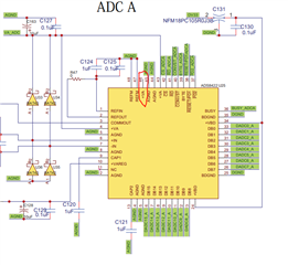
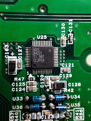
I have a problem operating ADS8422 ADC. I attached the schematic I am using and the mounted ADC picture. All the control signal is from FPGA, and FPGA also reads the digital output of ADC. Attached is the timing diagram for the ADC. I know the wait time after the PD2 pulled up is 25 ms. As the program goes on, the data that I captured is after more than 25ms. The FPGA I am using is cyclone 5 with a 3.3V supply. The problem is

  1. What I am getting from the ADC output is high at all times.
  2. I measure the REFOUT at pin 2 using a multimeter, but the output is 0V.
  3. COMMOUT also produces 0V.

It is like the ADC is not turning on. Kindly help me with this. Let me know what I should do.

Thank you very much.3750.ADC_schematic.pdf

  • Hello Mohd,

    You are missing a +VA connection to your VA_ADC power supply.

    Also, the REFOUT and COMMOUT pins will measure 0V if the device is in shutdown.  The /RESET/PD1 and /PD2 pins must be high for the REFOUT and COMMOUT pins to be active. 

    Also, the digital ground (DGND) and analog ground (AGND) must be connected together at some point, preferably next to the ADC device.  I do not see a common connection between these grounds on your attached schematic.

    Regards,
    Keith Nicholas
    Precision ADC Applications

  • Thank you for your reply.

    Can I ask, all the VA inside the ADC are not internally connected? Any problem if I missed this connection? I was referring to the terminal function in the data sheet and only saw two links for VA. So I assume I already make the connections.


    For the AGND and DGND, I have already connected them.


    I gave PD1 and PD2 HIGH, as shown in the timing diagram I shared in my previous inquiries.

    Thank you very much.

    Shukri.

  • Hello Shukri,

    Typically, each power pin is connected to different parts of the internal circuitry, and are not connected together internally.  It is likely a section of the device does not have power, and thus, would not operate correctly.

    The terminal function table should list pin 43 as a +VA connection, to match the pinout of the package.  I suggest connecting pin 46 to the VA_ADC net and verify.

    Regards,
    Keith

  • Dear Keith,

    Thank you very much for your reply.

    It will take some time for me to modify the board and connect pin 46.

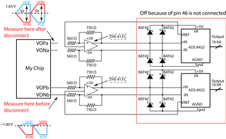
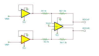
    However, while debugging, I have another question. The VOP and VON output from my chip connect to THS4131 seem weird. I measure this output directly at the output pin of my chip, connecting to the resistors 560, 750, and THS4131, as shown in the illustration attached.

    Therefore, I disconnect the output from the amplifier; as shown in the illustration, it seems fine. So, I wonder if my buffer is enough to drive the amplifier.

    Or is it maybe because the ADC is off and there is no REF OUT to the amplifier?

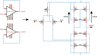
    Here I attached the buffer amp, and it is current. Is it sufficient to drive the amp?

    Or the way  I measure is wrong? Thanks in advance for your opinions. Your help is kindly appreciated.

  • Hello Mohd,

    Yes, it appears that your IC is not able to drive the THS4131 inputs.  Since the ADC is not powered up, the output common mode for the THS4131 will default to 1/2*supply, or for +/-5V supplies, it should be close to 0V.  When the ADS8422 is operating correctly, the output of the COMMOUT pin should be 1/2*Vref, or 2.048V.  This will change the load seen by the output of your IC, and may help or make it worse.

    You may need to add an additional buffer between your IC and the THS4131 inputs if this is the case.  Right now, in order to drive 3V differential, the current output needed from your IC will be around 5mA.

    Regards,
    Keith

  • Dear Keith,

    The ADC now work after I connect pin 46.

    However, as I mentioned before, the output of my chip is small when connecting to THS4131 through resistors 560,750. Probably the buffer of my chip cannot drive the amplifier because of the current leak through the 560 and 750 resistors.

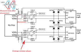
    Do you think if I maintain the same ratio but higher resistance value, such as I can overcome this problem instead of 560 and 750, I change to 100k and 130k? With this, smaller current leakage and probably larger swing? Also wonder the THS4131 can work?

    Thank you very much,

  • Hello Mohd,

    The input bias current for the THS4131 is 5uA, which would result in 0.5V of additional offset when using 100kohm feedback resistors.  In addition, the feedback resistor interacts with the input capacitance of the device, creating a phase shift in the feedback which can cause amplifier instability.

    Realistically, the maximum resistor values that should be used will be 1kOhm or less; the preferred value for best performance is about 400ohm.

    Your best option is to add an additional buffer on the inputs to isolate the input impedance of the THS4131 from the source impedance of your sensor.

    Regards,
    Keith

  • Dear Keith,

    Thank you for your reply. It would take some time to redesign and fabricate the PCB.

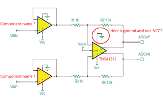
    However, can you please suggest the component's name as shown in the attachment?

    And also, for the THS4131, there is ground and not -VCC?

    Thank you very much,

  • Hello Mohd,

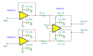
    Yes, the THS4131 will require a +/-5V supply.  Since your input voltage is +/-3Vpp with a common mode voltage of 1.65V, I suggest using the OPA2210 for the input buffers.  Below is a more complete circuit for the amplifier front-end.

    Regards,
    Keith