Hi,
I am using 4 x ADS1256 ICs on our board. 1st 3 ICs are configured to read one differential channel and 4th IC one is configured with 4 single-ended channels.
All differential channels are programmed for continuous cycling. Remaining single-ended channels programmed are using MUX cycling.
CLKIN is 7.68 MHz, SCLK is 1.92 MHz, DRATE is set to 3750 for both continuous cycling as well as muxed cycling.
The sequence of program for continuous cycling is:
1) Issue SDATAC command on the falling edge of DRDY.
2) Update STATUS REGISTER (hx00) on next falling edge of DRDY followed by delay of 5 micro seconds
3) Update ADCON REGISTER (hx00) followed by delay of 5 micro seconds
4) Update DRATE REGISTER (hxC0) followed by delay of 5 micro seconds
5) Issue SELFCAL command on the next falling edge of DRDY followed by delay of 5 micro seconds
6) Update MUX REGISTER (hx01) on next falling edge of DRDY
7) Issue RDATAC command on next falling edge of DRDY followed by delay of 8 micro seconds
8) Read DOUT (of 24 bits)
9) Continue to Read DOUT (of 24 bits) on falling edge of every DRDY
Observation & Issues on all 3 differential channels
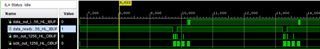
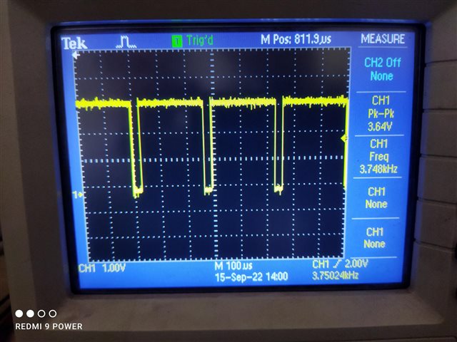
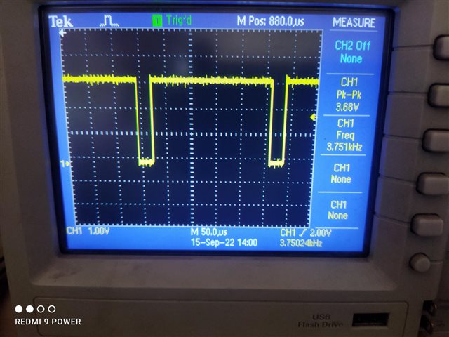
1) The desired DRATE is confirmed to be set on the oscilloscope with high time of 2.5 microseconds and remaining low for remaining period of DRDY period.
2) SCLK is being generated as per program sequence for 24 pulses with period of 0.52 microseconds
3) The DOUT remains high always because of which we are not getting readout properly. Kindly help us to resolve the issue
The sequence of program for MUXED cycling of 4th IC with 4 single-ended channels is:
1) Issue SDATAC command on the falling edge of DRDY.
2) Update STATUS REGISTER (hx00) on next falling edge of DRDY followed by delay of 5 micro seconds
3) Update ADCON REGISTER (hx00) followed by delay of 5 micro seconds
4) Update DRATE REGISTER (hxC0) followed by delay of 5 micro seconds
5) Issue SELFCAL command on the next falling edge of DRDY followed by delay of 5 micro seconds
6) Update MUX REGISTER (hx81 for 2nd SE-Ch) on next falling edge of DRDY followed by delay of 5 micro seconds
7) Issue SYNC, WAKEUP, RDATA commands sequentially followed by delay of 8 micro seconds
8) Read DOUT (of 24 bits) of hx80 1st SE-Ch
9) Update MUX REGISTER (hx82 for 3nd SE-Ch) on next falling edge of DRDY followed by delay of 5 micro seconds
10) Issue SYNC, WAKEUP, RDATA commands sequentially followed by delay of 8 micro seconds
11) Read DOUT (of 24 bits) of hx81 2nd SE-Ch
12) Update MUX REGISTER (hx83 for 3nd SE-Ch) on next falling edge of DRDY followed by delay of 5 micro seconds
13) Issue SYNC, WAKEUP, RDATA commands sequentially followed by delay of 8 micro seconds
14) Read DOUT (of 24 bits) of hx82 3rd SE-Ch
15) Update MUX REGISTER (hx80 for 1st SE-Ch) on next falling edge of DRDY followed by delay of 5 micro seconds
16) Issue SYNC, WAKEUP, RDATA commands sequentially followed by delay of 8 micro seconds
17) Read DOUT (of 24 bits) of hx83 3rd SE-Ch
Observation & Issues on all 3 differential channels
1) The desired DRATE is confirmed to be set on the oscilloscope with high time of 2.5 microseconds and remaining low for remaining period of DRDY period.
2) SCLK is being generated properly (as per program sequence during both read and write operations) 24 pulses with period of 0.52 microseconds
3) The DIN is found to be as programmed sequence.
4) However DOUT signal will not show up immediately after t6 delay after RDATA command instead shows up only during when DRDY is low i.e. when DIN is active. It looks like continuous mode is still active though first command issues was SDATAC. Please help us to resolve the issue.
We are struggling with these issues from quite some time. Immediate help will be appreciated.
With kind regards,
Somayya