This thread has been locked.

If you have a related question, please click the "Ask a related question" button in the top right corner. The newly created question will be automatically linked to this question.

ADC121C021: How to attach an external capacitor to VIN

Part Number: ADC121C021

Hi,

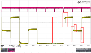
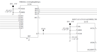
I am using a circuit that combines your TMUX1308QBQBRQ1 and ADC121C021QIMKX.
Is it possible to eliminate the external capacitor on the VIN side of the ADC121C021 and substitute a capacitor on the input side of the TMUX for the VIN capacitor?

In the image, I want to delete C139.

thaks,

Katsuya.

  • Hi Katsuya,

    The short answer is that it depends. Since this is a SAR ADC, you need to take into account input settling. What is the acquisition time you are running at? Please note that the input should be fully settled within 0.5LSB by the end of the acquisition time. With shorter acquisition times, this requires the use of an opamp+RC filter to help facilitate settling. Also, what is driving the MUX? schematic image seems to be cut off just left of the MUX. 

    Regards,
    Aaron

  • Sorry for the late reply.

    The acquisition time is 925us.
    The MUX switches channels every 1ms. After switching channels, it waits 925us before reading from the ADC, and data readout is completed 1ms after channel switching.

    The ADC is set to auto conversion mode.

    All voltages entering the MUX are MIN 0V to MAX 5V.

    A 12V voltage, a photo sensor output voltage, and other MAX 5V voltages are applied to the MUX input, all of which are held below 5V by a voltage divider resistor.

  • Hi Katsuya,

    With a larger acquisition time, the capacitor placed in front of the MUX should be fine. What are the voltage divider values? I would keep the resistor to GND as low as possible. Perhaps at 1kohms or less. The larger the source impedance the harder it is to settle the input. So if the resistor to GND is kept at 1kohms with the capacitor in parallel, you should be able to drive the ADC just fine. 

    Regards,
    Aaron

  • Hi Aaron-san

    The voltage divider resistor varies with the input voltage, and the resistance values on the GND side of the voltage divider resistor are 33 kΩ, 82 kΩ,

    and 100 kΩ.


    I took C139 of the schematic attached to the original question and checked the waveform, and found that noise is generated when the MUX channel is switched. Is this noise caused by GND being too large?

    Fortunately, there is no noise in the reading, but I am concerned about the cause.

    ch1:MUX output

    ch2:ADC I2C SDA

    Regards,

    Katsuya

  • Hi Katsuya,

    It it likely that the noise you are seeing is charge injection from the MUX. As long as the MUX output is stable and settled before the end of the acquisition phase, you should not see an error and that is likely why you are not measuring these transients. 

    Regards,
    Aaron