This thread has been locked.

If you have a related question, please click the "Ask a related question" button in the top right corner. The newly created question will be automatically linked to this question.

TI-JESD204-IP: Modifying TI204C-IP and figuring out clocks for the ADS54J64 and IP

Part Number: TI-JESD204-IP
Other Parts Discussed in Thread: ADS54J64EVM, ADS54J64, LMK04828

I have started modifying the zc706_8b10b reference design so that I can directly connect a ADS54J64EVM to the ZC706 but I have run into a few issues. I plan to use the ADS54J64 is mode 0 (LMFS = 4841) and set the sampling rate to 280MSPS, which makes the output of the ADC 70MSPS due to the 4x decimation.

My questions/issues are:

1. The sysref and clkin pins of the ADS54J64 on the ADS54J64EVM is connected to pins on the FMC that are no connects on the ZC706 board. Does this mean that the only way to provide these clocks to the ADS54J64 in this setup it to use the “ADS58J64EVM GUI” to configure the LMK04828 on the EVM board to provide 280MHz sampling clock? Do I need to do this everytime I turn on the boards? Are there instructions to be able to set the proper settings in the GUI because the ADS54J64EVM Manual.pdf does not explain this.

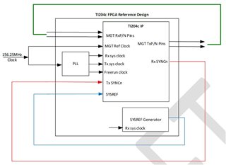
2. This and question 3 kind of go together. I am a little lost at exactly what the MGT REF CLK should be. Should this be at the sampling frequency or the ADC output rate? Should this be coming from the LMK04828 (FPGA_JESD_CLK or FPGA_JESD_Sysref) depending on what your answer is to my question 1? The user guide for this core just says “These must be connected to the MGTREFCLK pins of the FPGA”. The FPGA_JESD_CLK signal from the LM04828 on the ADS54J64EVM is connected to the FPGA’s MGTREFCLK0 pin through the FMC. Is that what this means?

3. What exactly should my line rate be set at. I found this equation, where M=# of converters, S=# of transmitted samples per converter per frame, N’= JESD204B word size, FC=frame clock, and L=number of lanes.

Lane Rate = (MxSxN'x10/8xFC)/L

For my application, M=8m S=1, N’=16, L=4 I believe. I think my frame clock is 70Mhz since I want to sample at 280MSPS and mode 0 has 4x decimation. Is this correct? If so, my lane rate should be 2.8GSPS

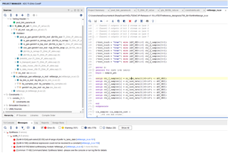
4. I have attached my modified jesd_link_params.vh, gtx_8b10b_rxtx.sv, and constraints.xdc files for reference. The only modification I made in the “7-series FPGAs Transceivers Wizard” for gtx_8b10b_rxtx is that I turned TX off in the “Line Rate, RefClk Selection” tab. I attached pictures of  the summary from the wizard for reference. With these modifications, when I try to synthesize, I get an error, which I also attached as a picture. I am not really sure why. I initially changed the NUM_RX_LANES to 4 within the refdesign_rx.sv file since that’s how many output lanes the ADC has. I changed it back to 8 and reran synthesis but get the same error. According to the ADS54J64 datasheet, the IQ data are on the same lane for each channel. My intention is to modify the reference design and the package the entire thing as IP to be used inside a larger project. Should I need be trying to package the entire reference design?


  • Since the forum will not let me upload the sv, xdc, or vhd files, I have attached the modified portion of the xdc as an image and pasted the changes I made in the other files below: 

    in gtx_8b10b_rxtx.sv

    module mgt_8b10b_wrap
    #(
    parameter IP_ID = 0,
    parameter GT_TYPE = "GTX",
    parameter NUM_LANES = 4,
    parameter NUM_QUADS = 1,
    parameter NUM_REFCLK_BUFFERS = 2,
    parameter TX_BYTES_PER_LANE = 8,
    parameter RX_BYTES_PER_LANE = 8,
    parameter GT_USERIO_IN_WIDTH = 16,
    parameter GT_USERIO_OUT_WIDTH = 16
    )

    In jesd_link_params.vh

    // The following parameter defines if the
    // IP is in 8b/10b mode or 64b/66b mode
    // Leave the second line commented if it is
    // in 64b/66b, else uncomment it to enable 8b/10b
    `undef IP_8B10B
    `undef IP_64B66B
    `define IP_8B10B
    //`define IP_64B66B

    `undef IP_TYPE
    `define IP_TYPE "RX"

    `undef ADC_RESOLUTION
    `define ADC_RESOLUTION 14

    `undef DAC_RESOLUTION
    `define DAC_RESOLUTION 14
    /////////////////////////////////////////////////
    // The following parameters configure the JESD IP
    // to interact with the transceiver created using
    // the Vivado Transceiver wizard.
    // Please ensure that the settings/parameters match
    // that of the transceiver
    /////////////////////////////////////////////////

    // Set the number of lanes in the link
    // This is equal to the number of lanes/channels
    // in the transceiver IP
    `undef NUMBER_OF_RX_LANES
    `undef NUMBER_OF_TX_LANES

    `define NUMBER_OF_RX_LANES 4
    `define NUMBER_OF_TX_LANES 4

    // Set the number of quads used in the transceiver
    // IP. This is based on the transceiver Quad/Lane
    // mapping. In this case, the 8 lanes are spread over
    // 2 Quads
    `undef NUMBER_OF_QUADS
    `define NUMBER_OF_QUADS 1

    // Select the type of Transceiver used in the IP
    // Options are: GTH, GTP, GTX and GTY. Refer to
    // the IP user guide for more details
    // GTH : Ultrascale GTH
    // GTHP : Ultrascale+ GTH
    // GTY : Ultrascale GTY
    // GTYP : Ultrascale+ GTY
    // GTX : GTX in Zynq/Virtex/Kintex 7000 series
    // GTP : GTP in Artix 7000 series
    `undef MGT_TYPE
    `define MGT_TYPE "GTX"

    // Set the number of Reference Clock
    // Buffers used by the Transceiver
    // In most cases, there is one clock per
    // link, and the clock is internally routed
    // to the individual Quad/Channel clocking logic
    `undef NUMBER_OF_REFCLK_BUFFERS
    `define NUMBER_OF_REFCLK_BUFFERS 1

    // The following parameter controls the mapping
    // of the ADC lanes to the transceiver lanes
    // This helps account for any lane mapping mismatches
    // on account of the board routing
    // This parameter is from the perspective of the ADC
    // and is ordered as {LANE_N,...,LANE2,LANE1,LANE0}
    // For example a value of {3,1,0,2} will mean the
    // following:
    // 1> Lane 0 of ADC is mapped to Lane 2 of the transceiver
    // 2> Lane 1 of ADC is mapped to Lane 0 of the transceiver
    // 3> Lane 2 of ADC is mapped to Lane 1 of the transceiver
    // 4> Lane 3 of ADC is mapped to Lane 3 of the transceiver
    // NOTE: Ensure that the parameter below has as many bits
    // as the number of lanes on the transceiver
    `undef LANE_ADC_TO_GT_MAP
    `define LANE_ADC_TO_GT_MAP {3'd3,3'd2,3'd1,3'd0}

    `undef LANE_DAC_TO_GT_MAP
    `define LANE_DAC_TO_GT_MAP {3'd3,3'd2,3'd1,3'd0}

    // The following parameter controls the polarity
    // of the transceiver lanes. If the P and N differential
    // pins are inverted between the transmitter and receiver,
    // set the corresponding bit to '1'. If there is no inversion
    // set the corresponding bit to 0.
    // This parameter is from the perspective of the ADC
    // and is ordered as {LANE_N,...,LANE2,LANE1,LANE0}
    // NOTE: Ensure that the parameter below has as many bits
    // as the number of lanes on the transceiver
    `undef RX_LANE_POLARITY
    `define RX_LANE_POLARITY 8'b00000000

    `undef TX_LANE_POLARITY
    `define TX_LANE_POLARITY 8'b00000000

    // Set the width of the final lane data bus exported
    // by each lane of the Rx IP.
    `undef RX_LANE_DATA_WIDTH
    `define RX_LANE_DATA_WIDTH 32

    // Set the width of the final lane data bus exported
    // by each lane of the Tx IP.
    `undef TX_LANE_DATA_WIDTH
    `define TX_LANE_DATA_WIDTH 32

    // End of parameters related to the transceiver
    //////////////////////////////////////////////

    //////////////////////////////////////////////
    // The rest of the parameters configure the IP
    // for the correct operation of the 8b/10b data
    // link protocol
    // PLEASE NOTE: The parameters MUST be set based
    // on those of the transmitting device, without
    // which the link will not work or may display
    // intermittent failures
    //////////////////////////////////////////////

    ///////////////////////////////////////////////////////////
    // Parameters related to 8b/10b encoding
    // These parameters are ignored if 8b/10b is chosen

    // The following parameter sets the value
    // of the F (octets per frame) parameter of
    // the device. Refer to the device datasheet
    // for the values allowed.
    `undef RX_F_VAL
    `define RX_F_VAL 4

    `undef TX_F_VAL
    `define TX_F_VAL 4

    // The following parameter sets the value
    // of the K (frames per multiframe) parameter of
    // the device. Refer to the device datasheet
    // for the values allowed.
    `undef RX_K_VAL
    `define RX_K_VAL 16

    `undef TX_K_VAL
    `define TX_K_VAL 16

    // End of parameters related to 8b/10b
    ///////////////////////////////////////////////////////////

    ///////////////////////////////////////////////////////////
    // Parameter related to 64b/66b Encoding
    // The following parameter sets the value
    // of the E (multiblocks per extended multiblock) parameter of
    // the device. Refer to the device datasheet
    // for the values allowed.
    // This parameter is ignored if 8b/10b is chosen
    `undef RX_E_VAL
    `define RX_E_VAL 1

    `undef TX_E_VAL
    `define TX_E_VAL 1
    ///////////////////////////////////////////////////////////

    `undef RBD_COUNT_WIDTH
    `define RBD_COUNT_WIDTH 10

    // End of parameters related to deterministic latency
    ///////////////////////////////////////////////////////////

    ///////////////////////////////////////////////////////////
    // The following parameters are for the RX and TX BUFFERs
    ///////////////////////////////////////////////////////////
    `undef RX_BUFFER
    `define RX_BUFFER "NORM"

    `undef BUFFER_RATIO
    `define BUFFER_RATIO 1

    `undef TX_BUFFER
    `define TX_BUFFER "NORM"

    ///////////////////////////////////////////////////////////
    // Define if the SYSREF is generated on the FPGA
    ///////////////////////////////////////////////////////////
    `undef SYSREF_GEN
    //`define SYSREF_GEN

    //`undef SYSREF_TARGET_COUNT
    //`define SYSREF_TARGET_COUNT 8


  • Hi,

    We have received your response and we will get back to you in a few days.

    Thanks.

  • Keira,

    Attached is a file that shows how to setup the ADC to operate in the mode you are planning on using. The TI data capture board (TSW14J56) FPGA uses a reference clock of 280MHz. I am looking into what would be required for the JESD204C IP. Normally this is the lane rate / 40 but I will let you know. I think this IP is flexible enough to allow a lower frequency to be used as the LMK will not be able to provide this. The highest divider available is 32.

    The ADC uses the ADS58J64EVM GUI which is capable of setting the LMK to output all of the required clocks and SYSREF signals.  

    Regards,

    Jim

    8475.ADS54J64_LMK_CLK_DISTR_280MHz.pptx  

  • Hi Jim,

    Thank you for your response and attachment. I am not using the TI data capture board (TSW14J56) board, I am using a ZC706 Xilinx board and trying to use TI's JESD-IP core to read in data. Now that I understand how to set up the LMK from your attachment, I need to figure out what needs to be sent from the LMK to the JESD-IP core. Have you gotten anywhere with looking into solutions for my questions 2-4?

  • Hi Keira,

    Kindly refer to the port and attribute description of the JESD IP user guide, as there are a few things that can cause synthesis errors. The reference design is meant to offer an idea of how the IP can be configured, and changes to the header file will essentially result in the IP parameters and port widths getting modified. Similarly, reconfiguring the transceiver will change things at the transceiver entity. I am listing a few possible reasons for the errors:

    1> If the number of lanes is decreased to 4, the ADC lane mapping parameter will become 2 bits wide (per lane). As a result, the 3'd usage will cause a width mismatch.

    2> Similarly, the polarity configuration will become 4 bits wide (4'd instead of 8'd)

    3> I will recommend leaving RX lane data width to 64 bits instead of 32 bits (for now). I am not sure if you have done the same at the transceiver wizard.

    4> Please refer to section 6.1.1 of the user guide. The parameters of the gtx_8b10b_rxtx.sv file should be left unchanged. These are automatically inferred from the top level of the JESD IP.

    5> If you change the transceiver settings using the transceiver wizard, there is a chance that the entity of the transceiver changes. In that case, the gtx_8b10b_rxtx.sv file will need to get updated to account for this. This is unfortunately a feature of the Xilinx 7 series wizards, because it creates/removes ports instead of creating something that is parametrized.

    To address your question about the reference clock frequency, this is based on the changes you make in the transceiver wizard. The transceiver has an internal PLL that uses the reference clock to regenerate the line rate needed (to lock into the data stream from the ADC). Jim will be able to help you with the line rate and reference clock frequency settings, but these should match what is set in the transceiver wizard.

    At the end of the day, I will recommend ensuring that a simulation of your changes compiles and works cleanly. To do this, please retain the Tx as well as Rx, and create a testbench that connects Tx lanes to Rx, applies the reference clocks and forces and releases the resets of the JESD IP. It will be ideal to have a working simulation before you attempt a transition to FPGA synthesis and P&R.

    Once you have a working simulation, you can package the part of the design under the testbench and use it in your block design.

    Regards,

    Ameet

  • Hi Ameet and Jim,

    Thanks for the help so far but I never heard back from you on the things you said you would continue to look into for me. I have gotten further on figuring out some things on my own but would like for you to check my clock decisions. Again, I am using the ADS54J64 in mode 0, which means:

    K=16, L=4, M=8,F=4,S=1

    I also want a sampling frequency of 280MHz, which means the CLKIN pin on the ADS54J64 needs an input of 280MHz, correct? This makes my frame clock 70MHz since Mode 0 has decimation by 4, correct? If this is true, this makes my line/lane rate 2.8Gbps, correct? I used the equation in my first post to find this.

    For the ADS54J64, I also need a system clock to the device, which I believe is the same clock that needs to go to sys_clk of the TI_204c_IP. This I choose 2MHz based on Max sysref frequency = Lane rate / [10 * K * F * n] from this post https://e2e.ti.com/support/data-converters-group/data-converters/f/data-converters-forum/1054266/ads54j60-ads54j60. This seems arbitrary. IS there anything else I should be taking into account picking this frequency?

    Lastly, I need refclk for the TI_204c_IP, which Vivado only gives me options of 112MHz, 140MHz, 175MHz, etc. based on the Line rate of 2.8Gbps. Picking this also seems arbitrary. Is there anything I should be taking into account picking this?

    Thank you,

    Keira

  • Keira,

    You need to provide a 280MHz clock to SMA J12. You are correct about the serdes lane rate = 2.8Gbps.

    Max SYSREF rate = data rate / (K * N) where N is any whole integer. For your setup, the max SYSREF can be is 4.375MHz (70MHz / (16 *1)). With the instructions attached, I am using a value of 2 for N to set your SYSREF at 2.1875MHz. This setup will also send a 140MHz reference clock to the FPGA.   

    I am checking on your other IP questions.

    Regards,

    Jim

    ADS54J64_LMK_CLK_DISTR_280MHz_K_16.pptx

  • This is amazing! Thank you for the quick response. On slide 3 you say "Configure ADC for Mode 0", what exactly do I need to click on this screen? Do I go through steps 1-5 picking any frequencies since I will be changing them later on the LMK and low level tab afterwards? How does the trim frequency and Nyquist setting selection in step 3 affect ADC performance for my setup? 

  • Keira,

    See new slide 4 for how to set the Mode. By default the GUI sets the mode to Mode 0. Do you plan on using the LMK PLL as the clock source for your other frequencies or an external clock? This may get a little complicated as the engineer that created this GUI is no longer with TI and this GUI is not user friendly. If you let me know what sample rates and modes you want to test, I may be able to create new configuration files for you to try.

    Regards,

    Jim

    6740.ADS54J64_LMK_CLK_DISTR_280MHz_K_16.pptx     

  • Thanks Jim, that didnt really answer my question. I was asking about slide 3. Does it matter what buttons I click here? I do not plan on using the LMK for any frequencies besides the ones needed for the ADC and FPGA to implement the TI_204c_IP, which I think you have explained how to set. 

  • Keira,

    This tab is just for loading existing configuration files. In your case, you will need to make changes either using the LMK tabs, low level tab or loading new configuration files. 

    Jim

  • Jim, Thank you again. I figured that was the case but I wanted to be sure since you had it in your instructions. 

  • I think I have figured out where some of my clk assignment confusion is coming from for the TI204c IP. This picture for the reference design shows that the 156.25MHz ref clk is going to the PLL, which it is not. The ZC706 ref design uses the 200Mhz clk as system clk and sends that to the PLL. Going through the ref design, the 156.25MHz clk from the loopback card only goes directly to TI_IP_inst.

    This being said, the system clk in the ZC706 ref design is 200MHz. How was this chosen? The PLL in the ref design seems to be creating sys_clk=100Mhz and mgt_freerun_clock = 78.125MHz from this 200Mhz clock. How do I determine what these frequencies should be for my application of the TI204c IP?


  • Hi Kiera,

    The MGT Ref clock frequency is dependent on the values given in the drop down menu of the transceiver wizard. This is not dependent on the lane rate. 

    In regards to the rx_sys_clock, the frequency of this clock is again related to the encoding and lane data width. For 8b10b encoding and a data width of 64 the frequency must be equal to or greater than LaneRate/80. 

    The TI204c IP User's Guide provides clocking guidelines for each of these clocks. Please see section 6.4 of the TI204c IP User's Guide for more information. 

    Regards,

    David Chaparro 

  • Yes, I was reading section 6.4 of the TI204c IP User's Guide and thats why I was confused because the reference design provided does not match. The ref design uses a Serdes Lane rate of 6.25Gbps and a data width of 64 yet MGT Ref clock = 156.25MHz, which is  LaneRate/40.

    Also, I just want to point out again that the reference design diagram I shared above is not actually how the reference design is wired and should be fixed because the 156.25MHZ clock does not go into the PLL. 

  • Hi Keira,

    I believe you are confusing between the transceiver reference clock and the rx/tx_sys_clock inputs to the JESD IP. All of these are described in section 6.4 of the user guide. Kindly peruse all the clocks described in the various sub-sections, as they pertain to different functions of the JESD IP.

    1> The transceiver reference clock is fed directly to the transceiver and has no specific correlation to the lane rate. You can use any of the frequencies offered in the reference clock drop-down menu of the transceiver wizard. The high level connection of top level inputs to the transceiver is illustrated in the diagram in section 6.1. The details regarding the reference clock are in 6.4.2. The user guide illustrates the typical clocking topology present inside Xilinx transceivers, and mentions that the designer must follow the PLL range guidelines as specified in the relevant transceiver datasheet.

    2> The rx_sys_clock (described in 6.4.7) is the clock that has a dependency on the Line Rate. There is a lower limit that is related to the line rate and the data width of the transceiver lanes, but a higher frequency is also supported.

    3> The transceiver also offers its own extracted clock (mgt_rx_usrclk2), which can be used to feed rx_sys_clock. This can be used if deterministic latency is not required by the application.

    The zc706 reference design showcases the ability of the  TI JESD IP to work accurately even if rx_sys_clock is higher than the minimum required value (LineRate/80 in this case). This is mentioned in section 8.2 of the user guide. That said, there is a typo in the paragraph related to the zc706. The rx_sys_clock is listed as 156.25MHz, while the reference design is actually using 100MHz. The document will be edited to mention that the reference design uses an rx_sys_clock that is higher than the required value of 78.125MHz. I will also add the note that the zc706 reference design generates the rx_sys_clock and mgt_freerun_clock by using the oscillator supplied 200MHz clock directly from the devKit instead of taking the 156.25MHz clock from the FMC.

    To summarize, you design needs to have the following:

    1> An MGT reference clock that has a frequency based on what you select in the transceiver wizard

    2> An rx_sys_clock that is equal to or greater than LineRate/80

    Regards,

    Ameet