This thread has been locked.

If you have a related question, please click the "Ask a related question" button in the top right corner. The newly created question will be automatically linked to this question.

ADS1256: Noise in the ADC output with and without load cell

Part Number: ADS1256
Other Parts Discussed in Thread: REF5025, OPA350, TPS7A47, ADS1261, ADS131E08

Hi,

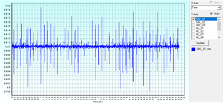
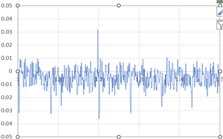
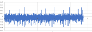
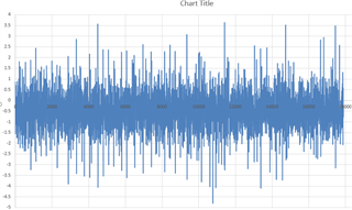
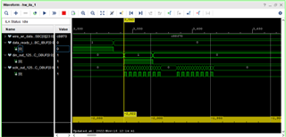
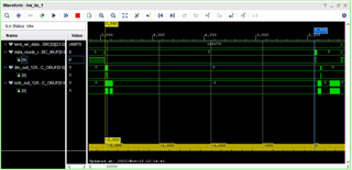
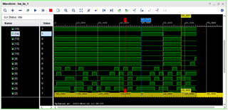
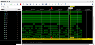
I am working on ADS1256 using Verilog code. I am reading the converted data in continuous mode. Current setup is with three differential channels connected and remaining kept open. The issue is I am finding noise glitches on the output with and without load on all the three channels. I tried even with shorting the inputs (ie 0V) for one of the differential channels. The issue is unchanged. Is that a common fact in this ADC? The sequence of operation I followed is: SELFCAL (after power-up), SDATAC, STATUS, ADCON, DRATE, IO_REG, SELFCAL, MUX, RDATAC (with loopback). The DREADY is as per the DRATE I had set. I even made sure that no glitches on SCLK. The master clock is at 7.68 MHz and SCLK is at ~1MHz. One of the images I had attached for reference of one of the differential channels. It is at DRATE 3750 SPS with PGA 64.

And, I tried with data rates of 100, 500, 1000, 3750, 7000, 15000 SPS and with PGA  64, 32, 8. Issue is the same. Is there any limitation in the ADC? I want the design to work at PGA 64 and DRATE at 3750 SPS. The schematic requirements are made sure as per the datasheet. Could you help me in resolving this noise at the output?

Thanks

  • Hi Prakash B B,

    Some questions for you and/or things to try:

    1. Do you have the buffer enabled?
    2. Do you have a very stable, accurate reference voltage for the ADC? If the reference voltage is moving around a lot, so will the ADC codes
    3. Can you send me the ADC register settings you are using?
    4. Have you performed a register read back to ensure that the register settings you are sending to the ADC are actually being applied?
    5. Can you try not enabling RDATAC mode and just using the RDATA command to request data from the ADC?
    6. Can you short the ADC inputs together by selecting the same input from the MUX register e.g. PSEL = AIN1 and NSEL = AIN1, then take 1000 samples at your desired data rate and gain, then send me this raw ADC data in hex? Please include the data rate, gain value, buffer setting, and reference voltage you used. You can also take more data sets for different configurations, but please make sure all configuration settings are included with each data set

    -Bryan

  • HI Bryan,

    Regarding your questions:

    1. No, buffer is not enabled.

    2. Yes, the potential is stable (Referenced at 2.5V).

    3. Registers are configured as: STATUS: 01h, MUX: 01h, ADCON: 06h, DRATE: C0h

    4. Yes, I did and found register values as: STATUS: 30h (not matching), MUX: 01h, ADCON: 06h, DRATE: C0h

    5. I sent even RDATA command also and found the same issue.

    6. I tried once by shorting both the inputs. But let me come back on the raw data with inputs shorted and send you the same.

    One more question, will there be any affect of resistor and capacitor values at the differential inputs? The values of resistor and capacitors are as mentioned in the datasheet page no. 28, Fig. 25 for differential inputs. But for VREF they are bit different like 100μF, 0.1μF, 4.7μF with resistance of 30 kΩ.

    Thanks

  • Hi Prakash B B,

    It might help if you send me your schematic. You can either post the schematic here or, if you do not want to share this information in a public forum, you can hover over my name, click "Request friendship" and then we will be able to share information via private message.

    Is the time scale accurate in the plot you sent in your original post i.e. seconds? The spikes appear to be repeating at slightly more than 100 ms, which implies some sort of external noise getting into your system. However this implies something very low frequency <10Hz. If this occurs even when the inputs are shorted, I would guess there is some sort of clock coupling on the digital lines or you have noisy power supplies. However in both cases I would have expected this noise to be higher frequency

    Please send me the shorted-input data as soon as possible so we can calculate the intrinsic ADC noise.

    -Bryan

  • Hi Bryan,

    I sent a request of friendship for sharing the schematic.

    The time scale is accurate. You are true on the spikes of <10Hz. I am attaching the raw data file for shorted inputs. Let me know on the same.

    raw_data.log

    Thanks

  • Hi Prakash B B,

    I accepted your request, please send the schematic whenever possible

    The data file you sent does not have any configuration information in it. What is the reference voltage, the gain, the data rate, and the buffer setting (I assume disabled after your previous comments)? We cannot calculate the noise without this information. Can I assume it is the same as you previously stated (3750 SPS, G = 64, VREF = 2.5V)?

    -Bryan

  • Hi Bryan,

    Thank you for your acceptance.

    I am extremely sorry for not adding the configurations. Since the configurations were same as previous message, I didn't add. It is true that the configurations are as mentioned by you i.e., Registers are configured as: STATUS: 01h, MUX: 01h, ADCON: 06h, DRATE: C0h, VREF=2.5V.

    Now, I hope I haven't missed anything.

    Thanks

  • Hi Prakash B B,

    Thanks for confirming the data.

    Can you perform one other set of "shorted input" tests? Instead of selecting the same input using the PSEL and NSEL bits, can you instead select two different channels and then bias them both to 2.5V (on your schematic I only see two channels anyway, PRIMARY_CH2P and PRIMARY_CH2N). I am hoping there is a test point at the output of your REF5025 / OPA350 that you can route to your analog inputs 

    Then take 1000 samples using all combinations of the following conditions: ODR = 30000 SPS, 3750 SPS, and 100 SPS as well as gain = 1, 16, and 64. This should give you 9 data sets of 1000 samples per data set.

    Can you take these measurements, put in a text document, and send to me? I want to see if there is a difference between shorting the inputs internally versus shorting them externally. I'd also like to see if gain or data rate have any affect on this issue. Please also make sure to label the different data sets with their appropriate configuration settings.

    -Bryan

  • Hi Prakash B B,

    We might need ~1 second of data under all circumstances, so maybe collect 32768 samples when the data rate is 30kSPS, 4096 samples when the data rate is 3750, and 128 samples when the data rate is 100 SPS. This should allow us to see if the 10Hz noise shows up for these tests as well

    -Bryan

  • Hi Bryan,

    I will surely send the data. Since it's a festival time here, you may get late response. Sorry for it. I will try to share in couple of days.

    Thanks

  • Hi Prakash B B,

    Ok, no problem

    -Bryan

  • Hi Prakash B B,

    Can you send me the power supply schematic as well via the private message? I would like to review this circuitry to see if it might have any impact on your measurements. Thanks!

    -Bryan

  • Hi Prakash B B,

    Thanks for sending the data over, can you also send the power supply schematic as per my previous request?

    I will review both and get back to you

    -Bryan

  • Hi Prakash B B,

    Thanks for sending over the power supply schematic. Nothing stuck out to me as incorrect. We us the TPS7A47 on a lot of our EVMs, so we know this is a good LDO to use.

    I reviewed the data you sent me, and I did not see any of the glitches you showed in the original data. The noise results were also very close to the datasheet values. Did you plot this data as well, and did you see any glitching? Maybe there is an issue in the way the data conversion calculations are being performed?

    If this is not the case, I think we can assume the shorted data is correct and that the ADC is working as intended. Therefore, we need to look elsewhere for the source of the glitching.

    What is the input signal you are applying to the ADC when you see the glitching? Is this from a precision source, from a sensor, etc.? Please provide as much detail as possible.

    In general, I would disable as much as possible on your board, then slowly start turning things back on to see if you can identify the source of the issue.

    Let me know

    -Bryan

  • Hi Bryan,

    Thanks for the response.

    I am sorry, I didn't plot the data. Let me check if I can find any glitches on the plot.

    The input fed is from the precision source i.e., from sensor. But it's in idle state (i.e., it's not varied). By connecting the sensor we tried finding the behavior of ADC and identifying the noise level to set our internal software gain. Whatever the data I shared is without varying the load, but just connected to ADC. Hope that should not result into noisy when under idle conditions.

    Sure, will go ahead in steps as you suggest and try identifying the issue. Meantime I will check with the raw data for glitches by plotting.

    Thanks

  • In addition:

    What is the best noise level for my design having specs: 3750 SPS, 2.5VREF, 64 Gain with buffer Off? In the data I shared can you make out the same?

    Because I found +ve as well -ve value of noise by looking at the data for the above specs. The ENOB should be 17.9 as per datasheet but I am not even close to it. If it is required to improve the ENOB what should be done?

    Thanks

  • Hi Prakash B B,

    I checked the noise for all of the data you sent me. For G=64, ODR=3750 SPS, buffer off, I calculated that the RMS noise was 0.855 uV and the ENOB was 17.5, which is very close to datasheet specifications.

    Regarding a precision source: typically I would not consider a sensor a precision source because a sensor can have inherent error and usually needs to be calibrated. A precision source is either benchtop equipment e.g. Data Precision 8200, or you can use a battery e.g. AA or AAA battery. A battery should give you ~1.5V output voltage, but that should be virtually noise free. This is a simple way to test if your system is working properly. If you are still seeing noise spikes even when measuring your battery, you probably have an issue with your board layout or power supplies.

    Let me know what you discover as you step through the troubleshooting process

    -Bryan

  • Hi Bryan,

    I had plotted the data shared with you for 3750 SPS, GAIN 64, 2.5 VREF and BUF_OFF. It is as attached, which shows glitches being seen.

    Let me know why am I getting those.

    Also, if you see the data has +ve as well as -ve values when both the differential inputs are shorted. Why is it so?

    Let me know on which all I should start removing (in schematic) in steps so that I can be free from these unwanted signals.

    Thanks

  • Hi Prakash B B,

    This is the plot I get when I graph your data (G=64, ODR=3750 SPS, buffer off). The x-axis is # of samples and the y-axis is in uV. This is different than what you are seeing. My plot looks like random noise, and when you calculate the RMS noise it is close to the datasheet values.

    Can you tell me what is the process you are using for converting codes to voltage?

    ADC noise should be largely random noise. Random noise has a Gaussian distribution around the input signal (ideally). When your input signal is 0V, that Gaussian distribution will be centered on 0V. Therefore, the magnitude of the measured noise will be >0V about half the time and <0V about half the time. This is why you are seeing very small positive and negative ADC codes.

  • Hi Bryan,

    Thanks for the plot.

    I didn't plot against the voltage conversation, but the direct raw data. Hope it is one another the same.

    What I need is the peak signals those are appearing like spikes ranging from -4.5V to 3.5V shouldn't be present. I need my noise to vary between -0.5V to 0.5V only. Is that possible? If so, how can I?

    Thanks

  • Hi Prakash B B,

    Are you plotting the decimal values then? Converting to voltage is just multiplying by a constant (4*VREF/Gain/2^24), so the plot should not look any different.

    I also do not understand your question about the signal "from -4.5V to 3.5V" (again, the plot is in uV). This is random noise, and it is within the range of the ADC noise floor. The only thing you can do to bring down the noise floor is average multiple samples together or just manually discard anything outside a certain range.

    You can also sample slower (which is similar to averaging multiple samples). But again, the noise of the data you have provided is close to what the datasheet specifies.

    -Bryan

  • Hi Bryan,

    Exactly. I just plotted decimal values of output. Since, it is multiplied by a constant, the plot will not be different as I feel.

    It's my bad. It is about the spikes having value between -4.5uV to 3.5uV if needed to be removed/discarded what best could be done? In HDL, is it possible to remove them by programming ADC?

    I am worried on the spikes those are appearing periodically.

    Another interesting thing I observed on ILA (Xilinx Vivado tool) (even on CRO too) that the DRDY is not going high immediately after SYNC followed by WAKEUP command:

    It is taking a time of 263 us (i.e., 2022x1/7.68M) to raise to logic 1 from the start of command and around 240 us after the command (which is supposed to be other way round). The above observation is with configuration 3750 SPS, 2.5 VREF, 64 Gain, ~2MHz SCLK, 7.68 MHz ADC CLK. And, after MUX command once, RDATA command followed by SYNC-WAKEUP and loop back to RDATA and so on. In the Fig. first signal is raw readout data, 2nd DRDY, 3rd DIN and 4th is SCLK. The plot is against samples not w.r.t. time. Each is sampled at 7.68 MHz. As per the datasheet (pg no. 20) DRDY pin is supposed to go high after the SYNC command followed by WAKEUP command and go low after 0.44 ms (t18) from the SYNC command. Would you let me know on this w.r.t. the behavior of my ADC?

    I found also that 16th bit toggles periodically at 58 to 60 ms. So, is it a read issue or the issue at AD conversion itself?

    Is there any limitation on read commands (RDATA, RDATAC) that I need to stop for sometime after certain duration?

    Thanks 

  • Hi Prakash B B,

    My previous post mentioned a few things you can do to reduce the noise, which basically is just sampling slower. The other option would be to use a lower noise ADC such as the ADS1261. The ADS1261 is the next-generation version of the ADS1256. At 4800 SPS and G=64, the ADS1261 has a noise specification of 0.34uVRMS. This is about half of the noise specified by the ADS1256.

    What is your actual SCLK speed? SCLK must be <CLK/4. So in your case SCLK must be <=1.92 MHz. Is that the SCLK speed you are using? The commands are not being interpreted correctly by the ADC so there must be an issue with the digital communication.

    Also please make sure the SPI mode (phase and polarity) are set as per the ADS1256 datasheet, which I have copied below. I can see that SCLK is idling so so that is good, not sure about the polarity though as I cannot tell when DIN is triggering

    -Bryan

  • Hi Bryan,

    Will look into ADS1261. And, will try using your suggestions for noise reduction.

    SCLK speed is 7.68MHz/4 i.e., 1.92MHz. But other commands are interpreted correctly. Why not these?

    Yes, the SPI mode is as per the datasheet only. SCLK is idle for the period as per the datasheet only.

    Another interesting thing I could observe on ILA with RDATAC. If one bit is toggled, others are also toggling. e.g. bit[14] is toggled and along with it bits [13, 12, 11, 10] are also toggled. Rest bits as I see they toggle because of noise. But, these 5 bits are toggling at the same time. Please refer the attachment (Fig. shows only required bits and remaining MSBs [15 to 23] are constant).

    Would you let me know the possible reason(s) for this toggling?

    Thanks

  • Hi Prakash B B,

    Have you met the timing requirements between the SYNC and WAKEUP commands, t11? This should be >=24tCLK periods. This does not appear to the be the case in your system.

    Regarding the toggling bits: this is just data coming out of the device. What are the decimal values associated with the data? And what signals are you measuring? This could very well be normal behavior

    -Bryan

  • Hi Bryan,

    I agree with you. I had just considered the WRITE period (4tCLK). My bad.Disappointed

    I am connected with a load cell, but not varying anything while measuring the behavior of ADC. And, its output varies between ±20 mV. I hope ADS1256 would be good enough to use for this device. Am I right? Since the output is low, we are targeting the gain as 64. Is there any better way than this? If I use with low PGA and program gain registers is that ok?

    The signal which is measured by applying a force (weight) of 25kN max gradually using this load cell is, the behavior of specimen and its various characteristics.

    Thanks

  • Hi Prakash B B,

    What do you mean by "good enough"? That is really something you need to decide. If you want <1nV noise, then no this ADC will not be sufficient (nor will any ADC for that matter).

    I would encourage you to review the information presented in our application note A Basic Guide to Bridge Measurementshttps://www.ti.com/lit/pdf/sbaa532

    You can also review the information on ADC noise in our Precision Labs training material: https://training.ti.com/ti-precision-labs-adcs

    This resources provide the necessary information to make the determination if the system you are designing is "good enough"

    -Bryan

  • Hi Bryan,

    No no. Mine intense was just to understand that I am in the right way. My device output varies between ±20 mV. Is that fine using this device for my application?

    I am trying to reduce the spike kind of outputs those are appearing in my design. Is it possible further to reduce their peak value by playing with coding (Verilog)? Or is it required some modifications on the hardware side?

    Thanks

  • Hi Prakash B B,

    The ADS1256 has a differential input range of +/-2*VREF/PGA. If VREF = 2.5V and PGA = 64, then you have an input range of +/-78mV. If your input signal is +/-20mV, the ADS1256 will be able to measure it. The input signals should also be within the absolute input voltage specifications in the datasheet, which change depending on the state of the buffer (on or off). For example, if AINP = 100V and AINN = 100.02V relative to AGND, then your differential signal is 0.02V (or 20mV). But 100V is well above the absolute input voltage limitations of the ADS1256, and would likely destroy the ADC.

    I had previously suggested some ways to try to reduce the spikes. Have you tried any of these? These are the only suggestions I have at the moment because it appears this is just random noise inherent to the ADC. If you are able to identify the source of any noise it might be possible to remove it. Please let me know if you do

    -Bryan

  • Hi Bryan,

    Thanks for the information.

    I tried increasing the averaging of samples. Which reduced the spikes to some extent. But the issue is I can't read them as fast as I wish since the SPS is smaller. I could get only this from the suggestions. I am also working on finding the other source of noise.

    How many parallel ADCs can be driven from the source schematic I had shared you before? Will the number of ADCs affect the noise performance of my schematic?

    Thanks

  • Hi Prakash B B,

    Yes, this is the tradeoff. Sampling slower will improve the noise at the cost of increased latency. If you can find the source of the noise it is possible you can try other solutions. For example, if the noise is coming through the input, you could heavily filter the input e.g. with a low cutoff passive filter or even an active filter. The tradeoff with this approach is that a filter with a low cutoff frequency has a long settling time, so if the input happens to change quickly it will take a long time for the voltage at the filter output (ADC input) to reach a steady state. Also, if the noise is not coming through the input, more input filtering will not help.

    The number of ADCs you can sample in parallel depends on the drive strength of your controller and the amount of capacitance on the SPI bus. If you wanted lots of ADCs on the same SPI bus, you would also be limited by the number of SPI peripherals / GPIOs to actual control the ADCs. There are workarounds for some of these issues such as adding logic buffers to help increase the drive strength of the system, or IO expanders for more GPIOs.

    As far as noise, you theoretically should not see any noise degradation from having multiple ADCs in parallel. However, this will complicate the actual PCB layout and routing, which could introduce noise that would otherwise not be present in a single-ADC system. So just be careful

    -Bryan 

  • Hi Bryan,

    Agreed to the tradeoff. Currently I am working on identifying the source of noise. Once done will try to eradicate or reduce to an extent required for our design.

    In the design, we have different SPI buses for 3 ADCs. So, there will not be an issue of driving strength of the controller. Noted your workaround suggestion if in case same SPI is driven by multiple ADCs.

    Surely will take care of routing and PCB layout.

    Thanks

  • Sounds good Prakash B B, let us know if anything else is needed here

    -Bryan

  • Hi Bryan,

    Definitely. I need an information what if I reduce the operating frequency of ADC to 2-4 MHz instead of 7.68 MHz? Will there be any affect on performance?

    We are adding/removing component(s) by component(s) and trying to identify the noise issue. Let's hope for the best.

    Thanks

  • Hi Prakash B B,

    Reducing the ADC clock frequency should not have any effect on the performance. However, the ADC output data rate scales with the clock frequency. So if you are using 3750 SPS at 7.68 MHz, and then you set the clock frequency to 1.92 MHz, the data rate will now be 3750 / 4 = 937.5 SPS.

    Also please make sure to scale the SCLK frequency accordingly.

    -Bryan

  • Hi Bryan,

    That I observed and noted from the datasheet. Thanks again for reminding it.

    I think we are just closer in identifying the noise issue. Soon will close it. I will let you know on the same.

    Thanks

  • Hi Prakash B B,

    Okay, let us know what you discover

    -Bryan

  • Hi Bryan,

    The issue was crystal. We were driving 3 different ADCs with different crystals but same frequency (7.68MHz). When we were reading the data one after the other those unwanted spikes were appearing on all the 3 channels. After driving them through single crystal or using clock from FPGA we didn't find those periodic spikes. Right now I am trying to reduce noise level further if possible.

    Thanks

  • Hi Prakash B B,

    I am glad you were able to find the source of the noise, I know this can be frustrating. But at least now you are able to take action to eliminate those spikes

    Let me know if you need anything else, and thanks again for sharing your findings

    -Bryan

  • Hi Bryan,

    Sure. I may need your help till our product gets launched. I will keep pinging you now and then.

    Thanks

  • Hi Prakash B B,

    Okay, sounds good. I will close this thread then for now

    If you have additional questions, please start a new thread and we will support you there

    -Bryan

  • Hi Bryan,

    Thanks for your support.

    One last question in this thread: would you suggest any ADC similar (ie programming) to ADS1256 but having 8 or more  channels with simultaneous sampling and resolution of 24 bits or more?

    Thanks

  • Hi Prakash B B,

    The closest ADC we have to the ADS1256 that has similar performance, etc., but has simultaneous sampling is the ADS131E08.

    If you have additional questions about the ADS131E08, please start a new thread and we will support you there

    -Bryan

  • Hi Bryan,

    Thanks for the information.

    Surely will create a new thread. Thanks for having patience response.

    We can close this thread.

    Prakash