Because of the Thanksgiving holiday in the U.S., TI E2E™ design support forum responses may be delayed from November 25 through December 2. Thank you for your patience.

This thread has been locked.

If you have a related question, please click the "Ask a related question" button in the top right corner. The newly created question will be automatically linked to this question.

ADS1256: Sensor Output loading when Connected to ADC Input

Part Number: ADS1256
Other Parts Discussed in Thread: ADS1262

Dear Sir/Madam,

We are measuring millivolts from Pyranometer sensor (*solar radiation sensor) , model: LP Pyra 03 AV. But when we connect the sensor on the ADC input, the sensor output voltage get disturbed. for example the output voltage of the sensor when measured with Multimeter it shows 350mV but when connected to ADC it drops to 14mV. Although if we give a fixed mV signal from a calibrator instead of sensor to ADC input then it shows the correct mV reading. For confirmation we also have ADC1262EVM board and on connecting the same sensor it shows the correct voltage as shown in multimeter, here we have not observed any distortion in the sensor output or any kind of loading.

On comparing the Input circuit with ADC1262EVM board, its seems like the input signal is directly connected to ADC input.  Kindly have a look on the attachment file for schematics of our ADC board. 

ADC software configuration steps:

ADS1256_reset();
HAL_Delay(100);

ADS1256_WaitDRDY();
ADS1256_SetDiffChannel(adcChannel);

HAL_Delay(100);

ADS1256_WaitDRDY();
ADS1256_WriteReg(REG_DRATE, 0x13); // 10Sps
HAL_Delay(1);

ADS1256_WaitDRDY();
ADS1256_Sync();
HAL_Delay(1);

ADS1256_WaitDRDY();
status = readRegister(REG_STATUS);
HAL_Delay(1);
ADS1256_WaitDRDY();
mux = readRegister(REG_MUX);
HAL_Delay(1);
ADS1256_WaitDRDY();
dr = readRegister(REG_DRATE);
HAL_Delay(1);
ADS1256_WaitDRDY();
adcVal = readADCValue();
val = (adcVal & 0x7FFFFF);AFE-01.pdf

Do we have to add more configuration into it like activating Buffer & sensor detect etc.?

I am also attaching the schematics of our Analog Front end Circuit,  kindly let us know what we are doing wrong. 

Thanks & Regards,

Harinder SIngh

M2MLogger

  • Hi Harinder,

    If the sensor you are using has a large output impedance, you might need to enable the buffer in the ADS1256 in order to avoid loading. This appears to be the case for your system, as I at least see a 10k/10k resistor divider on the input channels. Please enable the buffer and see if the issue goes away

    Please note that when the buffer is turned on in the ADS1256, the absolute input voltage limitations change. The datasheet clearly describes this in the Electrical Characteristics section.

    -Bryan

  • Dear Sir,

    Thanks for your response!

    As per your suggestions, I have done the following modifications on the input circuit & code:

    1. Connected the sensor on the Differential Input configuration of U24 ADC IC, between AIN0 & AIN1. (*Its have only one 10K ) 

    2. Removed the 10K resistors (*i.e. R180/R182) so that signal goes directly into ADC. (*Buffer Enable seems to effective only after removing the resistors)

    3. Activated the Buffer in Status register (*by writing 0x02 into status register)

    But, loading is still there for example when I measuring the sensor output with multimeter its 170mV but on connecting at ADC input its shows 70mV if buffer is enabled & shows 30mV when buffer is disabled.

    Sir, kindly let me know if I am missing something or doing anything wrong.

    Regards,

    Harinder Singh

  • Hi Harinder,

    How is the sensor biased? I understand the output voltage is small, but if the absolute voltage is outside of the ADC's input range that could cause issues.

    You said that buffer was only effective after removing the 10k resistors - what happened before you removed the resistors? It does not seem like the buffer was effective at all thus far, so I am curious what this statement means.

    -Bryan

  • Dear Sir,

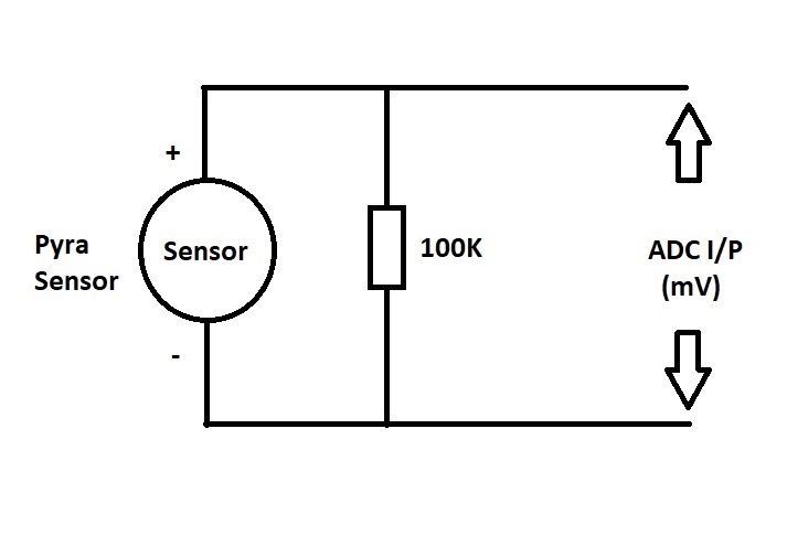
    1. How is the sensor biased? : Our sensor setup has silicon photodiode & 100k resistor, it doesn't need external excitation source, it gives output in mV. The output voltage is in range of the adc and this setup works fine with ADS1262 EVM board.

    Sensor Setup

    ADS1262 EVM Output: Its shows around the same voltage output that we are reading with multimeter  ~216mV. 

    2. You said that buffer was only effective after removing the 10k resistors - what happened before you removed the resistors? : 10K was causing Loading of the sensor, So the effect of enabling the buffer is not seen in actual. but on removing the loading effect is decreased but not gone completely. like I have said the normal output is 300mV when measured with buffer enable it shows 170mV and without buffer it shows 14mV.

    Its very strange thing we are not able to understand the issue so far. Any suggestion regarding the ADC configuration do we need to adjust the gain or other parameter.

    Thanks & Regards,

    Harinder Singh

  • Hi Harinder,

    I looked up the sensor online and found the following wiring diagram. If this matches your sensor, can you tell me the supply voltage you are applying to the sensor as well as the output voltage range? I see options from 0-1V, 0-5V and 0-10V

    In this modified circuit, is the negative input channel (AINP) connected to ground or is it floating?

    -Bryan

  • Dear Sir,

    We came to know about this issue when we first integrated the sensor with our system, but anyhow we don't have the same sensor with us so we reproduced the issue with this setup (*Diode + resistance).

    we have connected the sensor as per user manual and gives correct mV output when measure with multimeter but not with the ADC. Sensor was supplied with 12v supply.

    Regards,

    Harinder

  • Hi Harinder,

    The ADS1256 cannot measure certain voltages, so I am just trying to understand what you are applying to the ADC's inputs.

    For example, if the differential output of the sensor was 0.1 V, but the absolute voltage on one output pin was 10V and the absolute voltage on the other output pin was 10.1V, you could not apply this voltage directly to the ADS1256

    Also, with the buffer enabled, the ADS1256 might have trouble reading ground-referenced signals since the minimum absolute input voltage with the buffer enabled is exactly 0V. Any variation in this voltage might cause the ADC to give incorrect readings, even if the multimeter is capable of reading these voltages.

    I would try applying voltages to the inputs of the ADS1256 using a precision source and see if the ADC converts these correctly. You can try with the buffer enabled and disabled and see what happens. At least this will help identify where the issue lies, and help remove some variables from the system.

    -Bryan

  • Hi Bryan,

    "I would try applying voltages to the inputs of the ADS1256 using a precision source and see if the ADC converts these correctly. You can try with the buffer enabled and disabled and see what happens. At least this will help identify where the issue lies, and help remove some variables from the system." : We have tried your suggestion and give the source signal to ADC from a calibrator device, found that the adc count is more stable when Buffer is OFF but on Enable the buffer its give non linear response. Adding the comparison chart for your reference.

    Although if keep the input at fix voltage and measure the current in series we get current reading as per internal impedance of adc.

    Thanks & regards,

    Harinder Singh

  • Hi Harinder,

    Can you provide a table that summarizes the results you saw? The different inputs you applied, buffer on/off, etc.?

    If you apply 1V to AINP and tie AINN to ground with the buffer enabled for example, you will likely get a nonlinear response at the output due to the input limitations on the buffer. This seems to match what you are seeing, and is described at the very beginning of the electrical characteristics section on page 3.

    In this case, you would want to bias AINN to a higher voltage e.g. 1.5V, and let AINP swing around this voltage like a pseudo-differential measurement. Try this type of measurement and let me know if the output is more stable

    -Bryan

  • Hi Bryan,

    Thanks for your suggestion, I am adding more observations so that we can troubleshoot the issue.

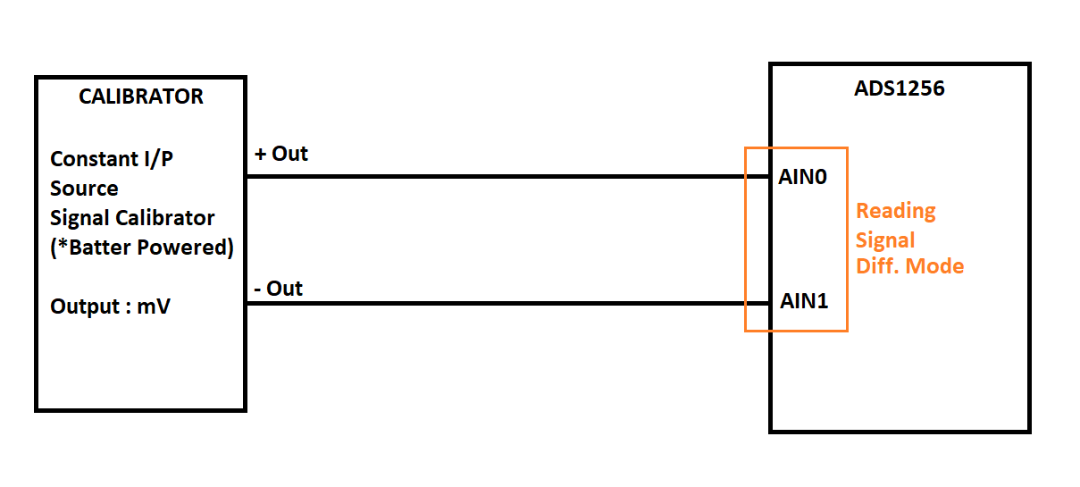
    1. Description of testing setup : Signal in mV is provided from calibrating device which is battery operated (*Its ground is not same as of ADC), calibrator is device which gives highly accurate mV signal. The signal which we are getting from calibrator is feed into ADC input at channel AIN0 & AIN1. We are reading the signal in the Differential configuration. Adding the Diagram for better understanding.

    2. Modification in the ADC circuit : Components marked as red are removed to simplify the things we have added 100K resistor at the place of C132 to provide GND reference. 

    Earlier we have used 10K for Proving GND ref. but observed its have more loading effect. 

    Q1. What should be the correct resistance value to provide the GND  Reff. at the ADC input ?

    3. "Can you provide a table that summarizes the results you saw? The different inputs you applied, buffer on/off, etc.?" : Adding the observation table for better understanding, input voltage is provided from calibrator

    Note : I am not able to understand why the ADC read data is more stable when buffer is off, after turning it on the read data starts floting +/- 10 points from the actual. ?


    4. We are running the Offset and Gain Self-Calibration (F0h) , do we also need to run System Offset Calibration command (F3h), which uses external source for calibration.

    Q2: Is the System Offset Calibration (F3h) is saved into memory of the ADC or we have to do it every time when ADC power up ? How to reset to factory default

     if changed?

    5. Plz go through the ADC init. Code that we using to get the binary data from the ADC, because we are not getting the correct binaries values if compared to the input voltage signal although it varies in same in same ratio as we varry the input, we are using 2.5V ref with the ADC . Kindly provide the step by step process to initialize the ADC before reading the raw bites, also please specify if any delay is required in between the steps. we are sure our SPI command request and response commands

    ADS1256_reset(); // send ADC reset CMD
    HAL_Delay(100);

    ADS1256_WaitDRDY();

    // Stop Read Data Continuous: CMD_SDATAC = 0x0F
    SendAdcCommand(CMD_SDATAC);

    HAL_Delay(10);
    ADS1256_WaitDRDY();

    ADS1256_WriteReg(REG_ADCON, 0x00); // Clk Out = OFF, Sensor Detect = Off, Gain = 1
    HAL_Delay(1);
    ADS1256_WaitDRDY();

    ADS1256_WriteReg(REG_DRATE, 0x13); // 5 SPS
    HAL_Delay(1);
    ADS1256_WaitDRDY();

    ADS1256_WriteReg(REG_STATUS, 0x02); // Buffer ON
    HAL_Delay(1);

    // Calibration Commands: CMD_SELFCAL = 0xF0
    SendAdcCommand(CMD_SELFCAL);
    HAL_Delay(10);
    ADS1256_WaitDRDY();

    // Set ADC MUX : Differential config. AIN0 & AIN1
    ADS1256_SetDiffChannel(adcChannel);
    HAL_Delay(500);
    ADS1256_WaitDRDY();

    adcVal = readADCValue();
    val = (adcVal & 0x7FFFFF);

    if (adcVal > 0x7FFFFF)
    {
    //take Bitwise invert and cap to 24bits
    int32_t valCompliment = ~val;
    int32_t valComplimentMasked = valCompliment & 0x7FFFFF;
    int valTwosCompliment = -1 * (valComplimentMasked + 1);
    val = valTwosCompliment;
    }

    volt_mV = (resolution * val) / 1000; // voltage in mV
    return volt_mV;

    Q3: Is the ADC init. steps are correct ? Any Delay to add in between? What could be the reason for not getting the correct binary data after giving RDATA command. 

    Kindly let me know if you need more information.

    Thanks & regards,

    Harinder Singh

  • Hi Harinder,

    I am not sure just adding a resistance will be enough, as that depends on how much current flows from the calibrator. I would either bias AIN1 to a specific voltage e.g. 1V and then apply the calibrator between AIN0 and AIN1, or you can potentially use pull-up / pull-down, where the pull-up is biased to 3.3V. This will keep the calibrator voltage output at approximately mid-supply, which is ideal for this ADC.

    The system offset calibration could be useful for your final system, but likely should not matter too much here assuming the calibrator is high accuracy.

    The initialization looks okay to me, assuming the SPI transactions are completing properly. But since you are reading relatively accurate data I would say everything is functioning as it should.

    Have you checked to make sure the differential VREF voltage at the ADC VREFx pins is correct? When you convert from code to voltage the assumption is that the VREF voltage is exactly 2.5V. If it actually is not, then the code scaling will be off.

    Can you check the VREF voltage, as well as send me the raw hex values received from the ADC?

    -Bryan

  • Hi Bryan,

    SPI transactions are working properly , as I am able to see the change in Mux & other commands working properly, Crosschecked this thing many times.

    1. I am not getting this Point :

    "The system offset calibration could be useful for your final system, but likely should not matter too much here assuming the calibrator is high accuracy."

    Q/s: If somebody have executed the System cal. command and nothing is connected at the input terminals then, will take the wrong calibration values correct? Is its reconfigurable to factory default if system calibration is modified ? Do the system calibration remains same or it resets on power cycle or ADC reset?

    2. Regarding VREF voltage : I have checked on the ADC its value is 2.491V. 

    3. Send me the raw hex values received from the ADC?

    Fig1: Buffer OFF : 1V input / Raw Value when combining the bytes : 1679435

    Fig2: Buffer OFF : 2V input / Raw Value when combining the bytes : 3356583

    Fig3: Buffer On : 1V input / Raw Value when combining the bytes : 1679807

    Fig4: Buffer On : 2V input / Raw Value when combining the bytes : 33525024

    Conversation Formula

    const double resolution = (double)(2 * 24910000/0x7FFFFF);
    val = ReadADC();
    volt_mV = (resolution * val) / 1000;

    Kindly let me know, if any thing to modify or change.

    Thanks & Regards,

    Harinder Singh


  • Hi Harinder

    Regarding calibration: the calibration is specific to the ADC settings for the self calibration commands. So if you perform calibration with the buffer on, the offset and gain calibration coefficients are likely not valid if you then turn the buffer off. As the datasheet says on pg. 24, you should perform a new calibration if the data rate, buffer configuration, or gain is changed.

    This also applies if you want to run a system calibration. The offset / gain calibration will be specific to the circuit connected to that input channel. If you change input channels, or change the input circuitry on the original channel, the calibration coefficients will likely be incorrect moving forward. For example, if you had a 1Mohm resistor in series with your input channel and performed the calibration, you would likely see a large offset calibration coefficient. If you then removed the resistor and did not perform a new calibration, the ADC output would be incorrect as the calibration coefficient still reflects the large offset from the 1Mohm resistor

    The ADC does not have a way to store this data for more than 1x channel / configuration settings at a time, so it would make sense to store this information on a per channel basis in your MCU, then write the OFC/FSC registers each time you switch channels or configuration settings. If you need to clear these registers completely, you can always power down the device, issue a RESET command, or simply write the default value to the OFC/FSC registers.

    Regarding the data you just took: when I converted the decimal values to voltages, I got the results shown in the image/table below. The results look very good and I don't see any issues here. Did you change the way you applied the input voltage at all? I am not sure what other help I can offer right now as it appears the ADC is operating as it should.

    -Bryan