This thread has been locked.

If you have a related question, please click the "Ask a related question" button in the top right corner. The newly created question will be automatically linked to this question.

ADS1299: SRB1/2 In-line Resistor?

Part Number: ADS1299

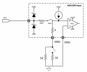
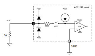
Previously, I was informed there is a in-line series resistance of 400 ohms on each channel input. In-line resistance on SRB1/2? 

My previous thread was https://e2e.ti.com/support/data-converters-group/data-converters/f/data-converters-forum/796333/ads1299-performing-impedance-measurement-using-the-lead-off-current-sources/2947070?tisearch=e2e-sitesearch&keymatch=%252520user%25253A70239#2947070

The image below was provided for each channel input. Is there a similar resistor on the SRB inputs?

Thank you,

Chris

  • Hi,

    I will need to discuss with the team and get back to you.

    Please allow around 24 hours.

    Thanks

  • Hi,

    There is only 150ohms resistor on analog input paths (not on SRB1/SRB2).

    But there is multiplexer switch resistance and significant routing resistance so at some point we approximated it(multiplexer switch resistance and significant routing resistance) to about 400oms.

    For SRB1/SRB2 there is no 150oms as other analog input paths, but routing resistance/ switch mux(i.e. the approximated 400 ohms) is still present.

    Thanks

  • After further investigation, it looks like the SRB2 resistance values are variable per channel. They do not seem to be constant across all channels like the analog inputs are. Is this true?

    I am assuming it is due to trace routing.

    channel 0 = ~275 ohms, channel 1 = ~325 ohms, channel 2 = ~175 ohms, channel 3 = ~250 ohms

    Does this make sense?

    Thank you,

    Chris

  • Hi,

    May I ask how do you make the measurement and the setup?

    In the meantime, I am forwarding your question to my team to discuss.

    Thanks

  • My first step is to identify the actually value of the current source, because it could be off by +/- 20%. I do this with two methods

    1) Enable the P current source and run it out of the normal analog inputs and through a 0.01% 5K resistor. I then tie the N channel to GND through SRB1.

    From this I can use your approximated 400 ohms plus my 5K to get the actual current value. I use that current value to measure various impedances connected to the analog inputs with high accuracy. I can get good measurements for all channels and keep the 400 ohms constant.

    2) Enable the P current source and run it through SRB2 and through a 0.01% 5K resistor. I then tie the N channel to GND through SRB1.

    With this method, I use my 5K value and the 400 ohm constant to get the actual current value. When I use that calculated current to measure the same various impedances connected to the analog inputs, the impedances are different across channels. I essentially worked backwards and identified the values mentioned above give me good results on the current value calculation and end up providing the same impedances as the first method.

    It seems that the SRB2 connection points for each channel has different impedances, and therefore results in different constants for each channel.

  • Hi,

    Thanks for providing the details.

    May I ask what might be the reasons or the driving goals you are doing this or what are you trying to chase down?

    Thanks

  • We are using the ADS1299 for impedance checking, but it needs to be very accurate. The 20% tolerance of the current source is not adequate, so we need to "calibrate" the current source before using it.

  • Hi,

    Thanks for letting me know.

    Just got back from the team -

    "    Yes it makes sense. Routing resistance is different for each channel."

    By the way, ADS device is not designed for both accurate and precise impedance measurement. It can detect some impedance change, but is not designed to be used for accurate and precise impedance directly.


    Thanks

  • Is it safe to assume it is constant across chips?

  • Hi,

    Probably not.

    It's usually suggested that customer may need to develop some calibration and/or correlation/regression algorithms/equations to meet the applications.

    Thanks

  • Hi Yang, 

    After some investigation and some development work. I am trying to calibrate (identify exact value of) the internal current source, but it seems to be not consistent. My circuit I have setup looks like the following.

    The switch on SRB2 is controlled by GPIO3 and places the second 5K in circuit on the second voltage reading attempt. This results in two equations (V1 = i * (5k + R) AND V2 = i * (2.5K + R) ). I can then solve for i.

    However, when doing so the values I acquire for the current source are different from the original ones I got from having the 5K connected to the IN1P (see image below).

    The second schematic provides more accurate current source values. Is there some current path I am missing on the first? I am effectively enabling SRB2 and removing the INP1 input from the circuit. Both use SRB2 to apply ground to the N side of the comparator.

    I would appreciate the guidance.

    Thank you,

    Chris

  • Hi,

    I don't recognize the 1st diagram you provided, is it edited from the diagram we provided earlier?

    May I ask why are there additional R and SRB1 and SRB2 there? Could you explain a bit more about your thinking process and testing approaches?

    -------------------------------------------------------------------------------------------------------------

    The abstraction diagram provided earlier, which is not listed in the datasheet, is a high level abstraction and may not 100% reflect to the real&exact design implementation. Also, there could be chip to chip fabrication variation, too.

    And, the Schottky diodes may also have slightly different leakage currents from chip to chip and/or fabrication to fabrications.

    Is there a way that you could remove the SRB1 to GND and do the voltage measurement?

    Because if the diagram is a reasonable abstraction, then if you connect the SRB1 to GND, that means both the inverting and non-inverting terminals of the OpAmp are all GND. In that case, I don't know how exactly the current may travel, which depends on the OpAmp's internal model and/or design.

    ----------------------------------------------------------------------------------------------

    Would you please let me know what are you chasing down and why do you need that?

    Are you trying to understand and figure out what are the "possible range" and "precision, tolerance" of the current from the "hidden current source" that is shown in the abstracted block diagram?

    What are the tolerance and/or precision may you need for that "hidden current" source?

    ----------------------------------------------------------------------------------------------------------------------

    Would you please let me know the above, and then, I can bring the questions and concerns for internal discussions.

    ---------------------------------------------------------------------------------------------------------------

    "By the way, ADS device is not designed for both accurate and precise impedance measurement. It can detect some impedance change, but is not designed to be used for accurate and precise impedance directly."

    Thanks

  • HI, 

    Yes, I did just edit the diagram that was provided earlier. The additional R before the SRB2 pin is for the unknown internal resistance of the chip within the path of SRB2. 

    My thought process here is to try and identify the actual current value of the internal current source. The datasheet says it could be off by about 20%. This would result in having inaccurate impedance measurements. I do understand the ADS1299 is not designed to measure really accurate impedances, but we have been able to get fairly accurate with measurements using the second diagram I sent. The problem with that design is it  required a switch for each analog input. Therefore, I am trying to add a single switch on the SRB2 input.

    I would envision if I used the first diagram then I should get an accurate reading of the current source given the voltage drop over the known high tolerance resistors (5Ks). We would like to get as accurate as possible. Maybe even 1% might suffice.

    I hope that makes sense,

    Chris

  • Hi,

    Understood that

    1. " is to try and identify the actual current value of the internal current source."   

    Comments: I will bring this back to the team to see if we have any info for this hidden/non-disclosed current source.

    2. " we have been able to get fairly accurate with measurements using the second diagram I sent. The problem with that design is it  required a switch for each analog input. Therefore, I am trying to add a single switch on the SRB2 input."

    Comments: Still not clear what the problem is if you already got fairly accurate measurement?

    Would you clarify a bit more on "The problem with that design is it  required a switch for each analog input. Therefore, I am trying to add a single switch on the SRB2 input."?

    Do you try to avoid using a switch?

    3. "We would like to get as accurate as possible. Maybe even 1% might suffice."

    Comments: Are you saying that you would like to have 1% tolerance(precision) for that hidden/non-disclosed current source?

    Please let me know, and I can bring this back to my team for discussion to see if there is some more info we can share/disclose.

    Thanks.

  • 1. " is to try and identify the actual current value of the internal current source."   

    Comments: I will bring this back to the team to see if we have any info for this hidden/non-disclosed current source.

    Comments: Thank you

    2. " we have been able to get fairly accurate with measurements using the second diagram I sent. The problem with that design is it  required a switch for each analog input. Therefore, I am trying to add a single switch on the SRB2 input."

    Comments: Still not clear what the problem is if you already got fairly accurate measurement?

    Comments: We have good measurements, but we require a switch on the output of every analog pin of the ADS1299 in order to switch in a resistor and switch out the patient. This can take up our PCB footprint, and therefore we are trying to reduce the number of components and add a single switch on the SRB 2 pin.

    Would you clarify a bit more on "The problem with that design is it  required a switch for each analog input. Therefore, I am trying to add a single switch on the SRB2 input."?

    Do you try to avoid using a switch?

    Comments: In the current design a switch has to switch out the patient and switch in a 5K resistor to identify the internal current source value.

    3. "We would like to get as accurate as possible. Maybe even 1% might suffice."

    Comments: Are you saying that you would like to have 1% tolerance(precision) for that hidden/non-disclosed current source?

    Comments: We would like to know the current source actual value as best we can. I think 1% might suffice. 

    Please let me know, and I can bring this back to my team for discussion to see if there is some more info we can share/disclose.

    Thank you again,

    Chris

  • Forwarded to other team for internal discussion, please allow us more time.

    Thanks

  • Hi, 

    After internal discussion, 

    The current magnitude of the current source is actually the DC lead off detection current source that you can select by ILEAD_OFF[1:0] bits from 

    00 : 6 nA

    01 : 24 nA

    10 : 6 µA

    11 : 24 µA

    But, again, as datasheet mentioned, the current magnitude has around 20% tolerance/variation.

    Thanks

  • Hi, 

    Thank you for the information.

    My primary issue is the current source measurements I am acquiring are different depending on the method I use (explained above in the diagrams). When simply connecting the known high tolerance 5K resistor on the channel inputs, I get very accurate current measurements of the 6uA current source when sending the current through the 5K and measuring the voltage drop across it. However, when I connected that same 5K resistor to the SRB2 pin and route the current source through SRB2 the current measurement is accurate on CH1, but inaccurate on the other channels (e.g. 2, 3, 4)

    It seems to me that there is some leakage current when routing the current source out of SRB2 pin vs. out of the channel inputs.

    Is there anything in the HW that is causing this?

    Thank you,

    Chris

  • Hi,

    Do you setup the resistor(s) and see if you could disconnect all other unrelated MUXes switches, and then the measure the current for only one channel at a time?

    May I ask how inaccurate when you say "....route the current source through SRB2 the current measurement is accurate on CH1, but inaccurate on the other channels (e.g. 2, 3, 4)"?

    And, when you say "inaccurate", does the current change/vary differently every time when you measure the current on the same channel?

    Or, is it just different across different channels?  And, is it more or less than 20% of the current setting?

    Have you tried other current magnitude?

    --------------------------------------------------

    From the datasheet

    9.2 Functional Block Diagram and Figure 18. Input Multiplexer Block for One Channel,

    the SRB1 and SRB2 can be configured to connect to the selected inputs terminal before the Low Noise PGAs by MUXes.

    And, after the SRB2 and before the Low Noise PGAs, there are many other muxes/switches that need to be taken care of and could also affect the current measurement as opposed to SRB1.

    Also, in the diagrams you modified/edited, there is one current source at the inverting terminal overlooked; please refer to datasheet Figure 36. DC Lead-Off Excitation Options (b)

    Thanks

  • Hi, 

    Do you setup the resistor(s) and see if you could disconnect all other unrelated MUXes switches, and then the measure the current for only one channel at a time?

    Yes, I did attempt to do that. I removed all switches and MUXes and measured a single channel at a time. I still had inaccurate results. 

    When I say inaccurate, I get 1% difference from 6uA when using the analog input channels. I get 3% difference when using SRB1. These calculations result in a measurement of a known 0.5K impedance on the analog channels to be either 0.506K(1%) vs. 0.569K (3%). 

    It does seem to remain constant through reboots and re-calibrations. Not sure if it is the same across multiple samples.

    We are unable to use a stronger current magnitude. We have to use 6uA for our application.

    I do have the other inverting current source disabled. 

    Here is another diagram to help frame what I am trying to do. Below, the red lines are the current way which seems more accurate. The blue lines are what I am trying to do, but seems to be more inaccurate. The blue uses two resistors because the internal impedance of the SRB lines are unknown. The channel inputs was estimated to be fairly consistent to be around 400ohms. 

    Thank you again,

    Chris

  • Hi Chris,

    Appreciate for your explanation. 

    For "..I do have the other inverting current source disabled.... ", 

    Do you use LOFF_SENSP and/or LOFF_SENSP to switch with connect the current source(s)?

    And, agree with that - "The blue uses two resistors because the internal impedance of the SRB lines are unknown." - as the blue line you are trying to do seems travel through mux(es), switch(es) and with longer path with branches/distraction as opposed to the redline seems to flow in a shorter path with much less branches/distraction according to the block diagram, but not sure on the silicon level/perspectives.

    I know you want to have 1%(unfortunately this is not within the datasheet spec) accuracy current source for your application and has been trying to measure it for V&V.

    Do you want to try flip the current source direction? How about change different resistor values?

    Or,

    Do you think you could use any equation(linear, curve fit or regression) in the firmware or software to achieve what you want to achieve, e.g. calibration first, and then do regression to the value or measurement you want?

    Please let me know what else I could help you here, and I can bring the questions to the team for internal discussion again.

    Appreciate

  • Hi, 

    Thank you again for helping me out with this. I am using the LOFF_SENSEP for my current source. I have tried flipping the source and I have tried different resistor values, but still no avail.

    From my experiments, it seems like the SRB2 path has more leakage current then the normal input channels. It is also more or less depending on the channel used with the SRB2 route. Because of the leakage, the current measurements that I am reading is not accurate when compared to the "red path" I showed earlier.

    If the path (red vs. blue) differences were purely resistive, then I would imagine I could derive the internal resistance and therefore equate the current from the original diagrams I showed above. However, because they are coming out distinctly different, it appears like there is leakage current that I cannot account for. 

    I will continue to pursue other options.

    Thank you,

    Chris

  • I am sorry about that. The things we have been discussing may not be commonly seen and usage for the chip, and it seems really down to the silicon level/perspective.

    Still enjoy discussing and interacting with you.

    Appreciate.