This thread has been locked.

If you have a related question, please click the "Ask a related question" button in the top right corner. The newly created question will be automatically linked to this question.

ADS8920B: SDO timing exceeding datasheet specifications

Part Number: ADS8920B
Other Parts Discussed in Thread: ADS8902B,

Hi there, 

We are using the ADS8902B ADC in one of our designs and would like to get some clarification on the timing of SDO.

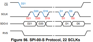
Below are screenshots from the ADS8920B datasheet:
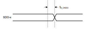
 (pg 11.)

 (pg 9.)

This is saying that new data will be ready on SDO at the latest 13ns after the CLK launch edge. 

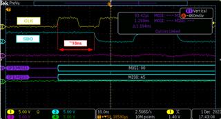
Below is a trace captured on our implementation of this ADC which shows nearly 18ns for data to be ready on SDO after the CLK launch edge. Our Master device is a STM32F746IG which requires that data be valid on MISO (SDO from ADC) 5.5ns before it is to be sampled. So we are violating that requirement at the moment. Our SCLK is 50 MHz

My questions are:

  1. Is there also minimum and typical values available for Td_CKDO in the ADS8920B datasheet? We are considering using Early Data Launch (EDL) mode on the ADC which will move the SDO 10ns (1/2 CLK) earlier. If Td_CKDO is only 7ns, will EDL move the SDO 10ns earlier to 3ns before the launch edge? The master would then be reading the previous data.
  2. Why is the ADS8920B taking 18ns to have data ready on SDO? This appears to be violating the datasheet spec of 13ns maximum.

 Best regards,

  • Hello Max,

    My apologies for the late reply.

    1.  There are no minimum or typical values available for Td_CKDO, however, it should not be anywhere near the 13ns maximum spec at room temperature.  Using EDL will simply launch the data 1/2 clock cycle earlier, but the delay time will remain the same (13ns max).  The idea for EDL is the ADC launches the data on the same clock edge that the host processor captures the data.  As long as the host processor does not require a hold time after capture, or hold time equal 0ns, then this mode will work well and allows more time for the clock edge to propagate to the ADC from the host, and for the data on SDO to be stable at the host MISO before the next host capture edge.

    2.  You did not state which SPI mode you are using.  On power-up reset, the ADC is in SPI mode 00.  In this mode, the MSB on SDO is launched on the falling edge of /CS, and the remaining bits are launched on the falling edge of SCLK (SDO launch edges are shown in BLUE in Figure 56).  If this is the mode that you are using, then the launch edge in your attached drawing will be the falling edge, and the actual Td_CKDO time is 8ns, which is a more reasonable typical value for this delay.

    For SPI, you typically will capture data on the opposite SCLK edge as the launch edge.  Since you are using a 50MHz SCLK, you cannot guarantee that the SDO data will be valid by the next SCLK edge, so using EDL should work in your setup, assuming there the hold time requirement for your host processor is 0ns.

    Regards,
    Keith Nicholas
    Precision ADC Applications

  • Hi Keith,

    Thanks for your reply. I misinterpreted Figure 56. We are indeed operating in 00 mode so the Td_CKDO is more like 7-8ns. We have tested with EDL mode and it seems to have solved the problem. With 50MHz clock (20ns period) and Td_CKDO is max. 13ns, we must use EDL to guarantee data is ready on the CLK rising edge for the master to sample.

    However I see an issue. Our Master (STM32f7) has "Data input hold time" of 4ns. Using EDL, the MISO hold time is defined by the Td_CKDO which ranges from 0-13ns. In our case, it seems to be 8ns but this could just as easily be 2ns, correct? In this case, we are violating the MCU timing requirements. 


    This leaves us in a tricky situation - use EDL mode and hope that Td_CKDO is always > 4 ns or not to use EDL mode and hope Td_CKDO < 4.5 ns (MCU MISO setup time is 5.5ns). This has already proven to not be the case. 

    Do you see any other solution to this other than decreasing the CLK speed?

    Best regards,

    Max

  • Hello Max,

    Yes, the Td_CKDO delay could be much shorter on different devices and could possibly be less than 4ns.  In any case, for a robust design, you need to assume 0ns minimum delay for the Td_CKDO specification.

    Keep in mind that the minimum delay observed by the host will be greater than 0, since you will have the board delay for the SCLK signal between the host and ADC and then the delay between the ADC SDO pin back to the host MISO.  This round-trip delay is already likely around a few ns total.  You can always add a small delay in either the SCLK path or the SDO path.  Adding a small RC filter (or just a series resistor in combination with the board and input pin capacitance) will also add additional delay.  Another option would be to add a single gate buffer, which can also add several ns of delay.

    The 'simplest' way to meet the spec is to slow down SCLK, but I am guessing that is not a good option in your system.

    Regards,
    Keith