Hi !
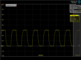
We are using the DAC8742H in HART mode and have configured XEN, CLK_CFG0 and CLK_CFG1 to accept an external CMOS clock source (generated with a function generator) running at 3.6864 MHz (line 1 in Table 1 on page 16 of the data sheet). In accordance with the description of this configuration, we have connected the CMOS clock between XTAL1 (X1, pin 28) and GND. The CMOS clock has a peak-to-peak amplitude of 3.0 V and an offset of + 1.5 V, so the logic low level is 0 volts and the logic high level is + 3.0V. Se screen shot #1.
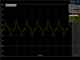
However, when we connect the CMOS clock in this way to pin X1, the clock signal as measured at this pin is level shifted up to IOVDD (+ 3.3V) and appears to be ac-coupled, see screen shot #2. Does this mean that the CMOS clock signal must be ac-coupled to pin X1? I can not see that the data sheet mentions this.
Have a nice day and thank you in advance for an illuminating answer !
Best regards,
Jan


