This thread has been locked.

If you have a related question, please click the "Ask a related question" button in the top right corner. The newly created question will be automatically linked to this question.

ADC12DJ2700EVM: baseline transient response

Part Number: ADC12DJ2700EVM
Other Parts Discussed in Thread: LMH5401EVM, LMH3401EVM, LMH3401, LMK04828, LMX2582

Hi everyone,

we have an issue with adc samples reaching a stable baseline after changing dc input level.
Following a detailed description:
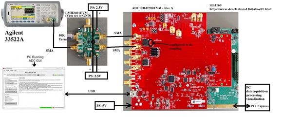
Hardware:
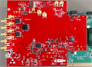
- Evalboard ADC12DJ2700EVM
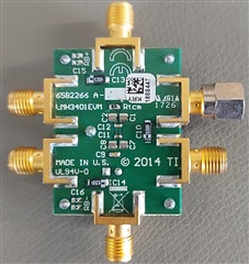
- Evalboard LMH5401EVM (CM input connected to GND)
- AWG square wave 50 second high, 50 second low (level like to see in sample data)

Setup with "ADC12DJxx00 GUI":
- Evalboard LMH5401EVM SMA IN+ driven from AWG square waveform (dc coupled), SMA IN- terminated 50 Ohm
- LMH5401EVM SMA Out +- connected to ADC12DJ2700EVM SMA INA+- (Channel A dc coupled)
- ADC clock 2.5 GHz (onboard generated)
- ADC analog input range default
- JMode 0 (single channel 5GSPS)
- ADC data format offset binary (data decimal 2048 correspond to differential input level 0V)
- One time ADC setup and started, continously free running sampling
- taking samples from adc data stream after certain delay
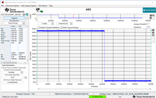
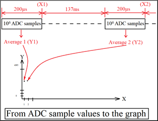
Data processing:
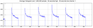
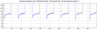
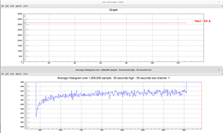
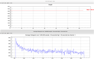
- each point along x-axis in diagram correspond to an average over 1 million samples (0.2ms trace)
- every 137ms one data point
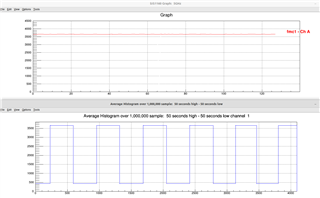
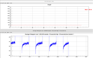
- AWG level adjusted to ADC data about decimal 3655 (high level) and 445 (low level)
- see picture screen4.png

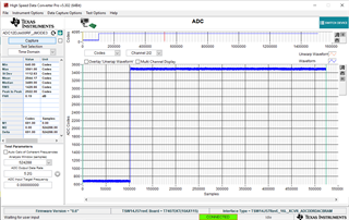
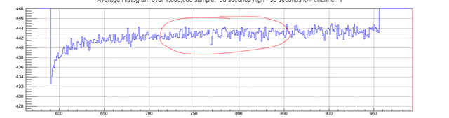
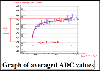
What we can observe:
- at the signal edge (rising or falling), the "Average data point" shows an overshoot
- see picture screen2.png and screen3.png


- like an capacitor charge or discharge curve, the "Average data point" needs some time (~1 Minute?) to reach a stable value (baseline value)
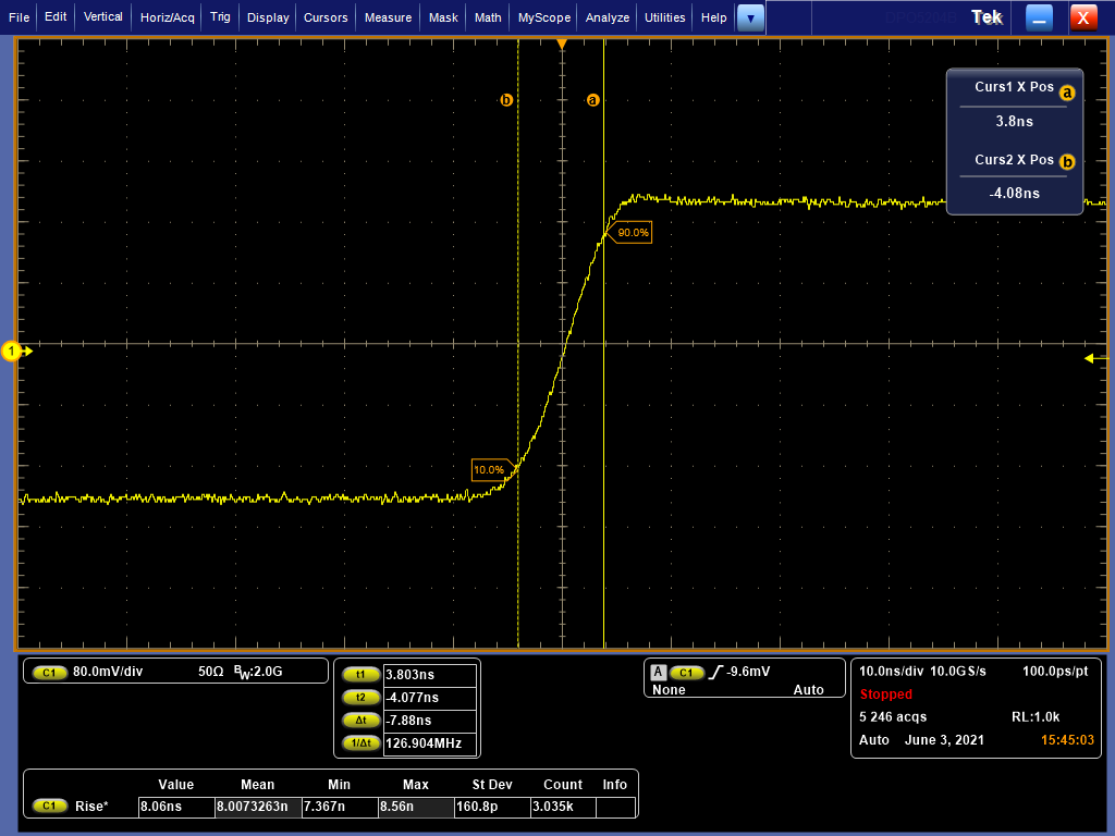
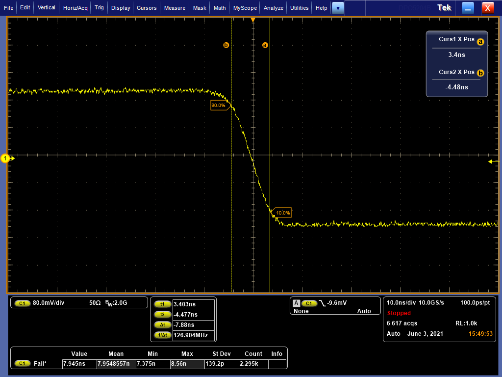
- zoomed in of overshoot region, see picture screen5.png and screen6.png


Can you confirm this behavior?
Can this be improved or avoided?


Best regards
Andreas

  • Hi Andreas,

    When putting in pulses to the LMH from an AWG, we would expect this. But to be sure, can you send us a few pictures or a detailed block diagram of the your test setup, complete with part numbers/model numbers, etc.

    Thanks,

    Rob

  • Hi Rob,

    thank you very much for your support.

    You meant that you would expect that, when pulses from an AWG were applied to the LMH.
    I would agree, if it were a few ns from the edge.
    The time to reach the correct level is in the range from 20 to 60 seconds in reality.

    We have also measured the signal at the ADC input with a 10µV resolution multimeter.
    The DC level between P and N is stable in less than 1 second.

    Part/model numbers of evaluation modules and the test setup are to be found in the pictures below.


    Board Rev. A

    Test setup:

    We have done additional measurements.
    You can see how the histogram mean value differs between a stable baseline (no level transition before)
    and a not yet stabilized baseline (after level transition).
    This is shown for 3 different baseline positions and transition directions.

    The ADC mode is always JMode0.
    The pictures are showing single channel and channel A/B histograms.

    High baseline after transition from low to high:

    High baseline no transition before:

    Low baseline after transition from high to low:

    Low baseline no transition before:

    Middle baseline after transition from high to middle:

    Middle baseline no transition before:

    Best regards
    Andreas

  • Hi Andreas,

    Thank you for the updates and I apologize for the delay.

    Can you measure with a DMM the input and output DC common mode voltages on the amplifier, when you have the AWG connected, etc in your test setup?

    Regards,

    Rob

  • Hi Rob,

    now we have the common mode measurement results of amplifier EVM.
    For the measurement we used a Beamax MC2 multimeter.

    1. Measured voltages to GND on LMH3401EVM with AWG Output 50s low + 50s high:

    AWG setting out low level -125mV
    IN+ = -125.5mV (from AWG)
    IN- = -78.7mV (50R terminated)
    Out+ = +181.63mV
    Out- = -199.12mV

    AWG setting out high level +125mV
    IN+ = 123.1mV (from AWG)
    IN- = 76.4mV (50R terminated)
    Out+ = -200.65mV
    Out- = +181.75mV

    Calculation of output common mode voltage:
    AWG setting out low level
    Vdiff = 380.75mV ; Vdiff/2 = 190.375mV
    VCM = OUT(+) - Vdiff/2 or OUT(-) + Vdiff/2
    VCM = -8.745mV

    AWG setting out high level
    Vdiff = 382.4mV ; Vdiff/2 = 191.2mV
    VCM = -9.45mV

    For the whole 50s low time and 50s high time of AWG Signal, the SMA Out(+/-) measured values were stable within +-50µV.
    Have a look in the video below too.
    It shows the Beamex from few seconds before to some seconds after switching of the AWG signal.

    2. Measured voltages to GND on LMH3401EVM with IN+ and IN- 50 Ohm terminated:

    IN- = -1.9mV
    IN+ = -1.55mV
    Out+ = -9.3mV
    Out- = -9.0mV

    Hope this helps.

    Best regards
    Andreas

  • Hi Andreas,

    Sorry for the delay, I am checking on a few things and will get back to you.

    Just so I understand from the measurements above:

    1. is with the AWG connected to the LMH device?

    2. is with the AWG not connected to the LMH device?

    Regards,

    Rob

  • Hi Rob,

    yes, that is correct.

    I should have mentioned, as termination we have used SMA Plug Termination 50 Ohm without Chain.

    Regards

    Andreas

  • Hi Andreas, 

    For the amplifier, what voltage do you have on the Vocm pin? If it is left to default it will be set to the mid-supply which will be 0V in the case of a +/- 2.5V supply. To properly match the ADC input, the Vocm pin voltage should be set to the input common mode voltage of the ADC. 

    Best, 

    Jacob 

  • Hi Jacob,

    Rtcm resistor of LMH3401EVM is set to 0 Ohm. So the output common-mode voltage control input pin CM of the LMH3401 is set to GND. I have measured 0V to GND at the CM pin. The measured output common mode confirms the setting at the CM input.

    The input common-mode voltage Vcmi of the ADC should be nominally 0V according to the datasheet. The LMH3401EVM GND is connected to the ADC EVM GND via SMA cables.  I think the measured LMH3401 output common mode voltage of -10mV matches well with the nominal input common mode voltage of the ADC.

    You could ask if the GND connection between the two EVMs via the two SMA cabel is too weak. However, we observe the described problem also on our own designed board SIS1354, where the LMH3401 GND and ADC GND is a common strong GND.

    Regards,

    Andreas

  • Hi Andreas,

    I agree, the ground connection between the two EVMs is fine and shouldn't be the issue.

    If you disconnect each EVM and measure the comment mode voltages, what to you measure for each EVM seperately?

    Thanks,

    Rob

  • Hi Rob,

    the common mode voltage for the LMH3401EVM without connection to the ADC-EVM is as already written above:

    Measured dc voltages to GND (IN+/IN- 50 Ohm terminated):

    IN- = -1.9mV
    IN+ = -1.55mV
    Out+ = -9.3mV
    Out- = -9.0mV

    Measured dc voltages of the open/unconnected ADC dc coupled input:

    1. before setup via USB (power on defaults)
    INA+ = 0.52mV
    INA- = 0.5mV

    2. after setup via USB (and after 10 minutes warm up)
    INA+ = 0.54mV
    INA- = 0.69mV

    All measurements made with Beamex.

    Regards,

    Andreas

  • Hi Andreas,

    I'm working with Rob and looking into this. We set up the LMH3401 with an ADC and found that it occurs when there is a coupling capacitor from the amp to the ADC.

    You mentioned that it was DC coupled, could you please make sure there are no AC coupling caps from the amp to ADC. The balun in that path could also be causing it.

    Also, could you please plug it to an oscillator and check if the charge/discharge artefact is still there. Some AWG may not be consistent at these low frequencies. If you try a little higher frequency, does it still have the same issue?

    Best regards,
    Ikram

  • Hi Ikram,

    the EVM ADC input is configured for dc coupling (R179/R180 = 0 Ohm and R1/R4 = DNI). There is no coupling capacitor or balun in the signal path. Please have a look at our pictures above. The signal shows for each 50s a dc level with less than 20% distance from ADC full scale.

    We measured the AWG signal dc levels with a very precise (Beamex) multimeter. Both dc levels are constant within <1s from the edge with an accuracy of +-50µV.

    We also made measurements with our own digitizer board SIS1354. The circuitry of the analog input stage and ADC is identical to the evalboards, additionally we can feed in a dc level at the LMH3401 with an offset DAC to adjust the ADC baseline. Instead of using the AWG we can generate the same signal with the DAC and observe the same effect.

    Many thanks for your support.
    Best regards,

    Andreas

  • Andreas, from our setup in the lab, these are what we found at 500 Hz with the signal DC coupled. 


    In your setup, could you please try setting your frequency higher and see if causes the same effect?

    - Ikram

  • Hi Ikram,

    thank you for measuring. You still have to change something to see the problem.

    1. Your picture shows a time interval of 100µs.
    We observe an effect that is only visible in the several seconds range.

    2. Your picture shows almost the whole level range.
    We observe a very small change of the DC level after the edge of about 10 to 15 ADC counts. For this you have to zoom to the dc level.

    Please, read the detailed description of the problem at the beginning of this thread and look at the pictures.

    To show the effect, we averaged 1 million samples for each data point in the graph. Then we had to zoom the amplitude to make the few counts visible.

    Best regards,

    Andreas

  • Hi Ikram,

    I would like to add something:

    We take the 1 million samples only about every 137ms (100ms programmed + something operating system time).
    Without averaging, the small dc level change would not come out the noise.

    regards,

    Andreas

  • Hi Andreas,

    Just to be clear, your concern is that you are sampling this granularity as circled below in the pic? Is that your issue?

    Regards,

    Rob

  • Hi Rob,

    >>Just to be clear, your concern is that you are sampling

    >>this granularity as circled below in the pic? Is that your issue?

    No !


    What we have noticed/measured is that the converted value for a DC level is not immediately constant after the input level has changed.

    We change the level at the input with a waveform generator every 50 seconds (10 mHz), so that we get sample values between appr. 440 and appr. 3650.


    Our measurement method:

    See the image below.

    About every 137ms we take 1,000,000 samples (200us) and then average them. We enter this average as a y-value in the graph at the timestamp X.


    A section of the first 13 seconds after a level change (sample value from ~3650 to ~440) can be seen in the graph/image.

    As can be clearly seen, the mean value only becomes approximately stable after about 13 seconds (decay time ~ 13 seconds).

    As you can see, the baseline shift is about 10 counts.

    If we perform the same test with a level change that is only half as large, then the baseline shift is also only half as large (~5 counts).


    Our problem is:

    1. that the "baseline" depends on the "history" (pulse high and pulse length)
    2. that if we move a baseline with a fed offset then we have to wait longer than 13-20 seconds to get a "correct" value for the baseline.

    We are talking about very small counts that are only detectable in Average mode, otherwise they are not visible in the normal noise of the ADC.

    But for our customer (application) this plays an important role.

    Best regard,

    Andreas

  • Hi Andreas,

    Thank you for all the additional details. This helps us start to understand the issue better.

    We will start to implement your specific setup in our lab. However, we still need some details.

    What is the sampling rate that you are using in JMODE0? Are there any additional ADC spi registers being set or modified?

    If so, please forward us those so that we can re-create the issue on the bench.

    Regards,

    Rob

  • Hi Rob,

    the sample rate is 5 GSPS. (2.5GHz clock)
    Configuration files clock:
    LMK04828_JMODE0.cfg (no modification)
    LMX2582_2500MHz.cfg (no modification)

    Configuration file ADC:
    ADC12DJxx00_JMODE0.cfg (something added)
    File is appended here.

    6457.ADC12DJxx00_JMODE0.cfg

    No more registers are modified.

    Best regards,

    Andreas

  • Hi Andreas,

    We are working on the script for testing this and we will get back to you early next week.

    Thank you,
    Ikram

  • Andreas,

    Can you measure the rise time of this pulse generator using an oscilloscope and report back?

    Thanks, Chase

  • Hi Chase,

    the rise/fall time is about 8ns for level 10/90%. Here are scopeshots of the measurements.

    best regards,

    Andreas

  • Hi Andreas,

    Thanks for letting me know about the rise time. Just a quick note regarding the status on our side. We've had a few discussions internally regarding how to approach this issue. As our evaluation platforms are not designed to take large data capture depths (such as 10^12 samples), there unfortunately is no easy way for us to measure this. Due to the architecture of our testing platform software, we are forced to be creative to find a method to replicate your measurements and this may unfortunately take some time.

    Which FPGA development kit are you using to perform these measurements? If possible and willing, it may be better for us to look at modifying your FPGA firmware such that it works with some development kit which we have access to, that is if we do not have access to your exact one.

    Thanks, Chase

  • Hi Chase,

    we can't take 10^12 samples at 5GSPS either!

    Please look again at the picture below:

    We take only 10^6 samples every 137ms.
    1 / 0.137ms = 7.3 times per second
    7.3 * 1.000.000 * 2 byte = 14.600.000 Byte/s * 8 bit = 117 MBit/s

    We chose the amount of 10^6 samples only to average out the noise. But this should be sufficient even with much less samples.

    Therefore I think your FPGA kit is suitable. So you only have to change the software a little bit.Smiley

    Of course, this also takes some time. Thanks for your support.

    Best regards,

    Andreas

  • Sorry,

    correct is --> 1 / 0.137s = 7.3 times per second

    regards,

    Andreas

  • Hi Andreas,

    I am aware and understand the timing. The issue is that our evaluation software is not capable of capturing and saving this much data within that 137ms window. And as a result, we are unable to capture the clusters of 10^6 samples sequentially. Unless a full FPGA application is created and dedicated to test this, we won't be able to capture the true settling time of a single cycle. We will have to try capturing along different segments of different cycles. Think of it as taking 10^6 from one cycle, taking the next 10^6 from maybe the 21st cycle, taking the next 10^6 from the 41st cycle, etc. As the settling overshoot you're experiencing is periodic, this approach would work. 

    But, unfortunately there is no easy way to trigger off external equipment in this manner, as we would be sampling the same ~200us of data following the trigger on each capture.

    Our challenge is finding a way to make our evaluation platform, which was never intended for fast/real-time captures, to sample a step function with rising edge similar to characteristics of your input source, but shift the hardware trigger at a periodic interval of 137.2ms exactly. This would allow capture of 10^6 samples of data for each portion of 137.2ms for roughly ~13 seconds (your settling time). We are still discussing possible solutions to replicate this.

    Thanks

  • Andreas,

    I think we can put something together like this so long as the period does not have to be an exact 137.2us. If this 7.3Hz sampling can sample at say 7.2Hz or 7.4Hz, I think we may have a solution to do this delay by passing the TRIGGER_OUT of the pulse generator through a microcontroller with code written to delay the TRIGGER going to our FPGA. I ask about the frequency being different than 7.3Hz as I'm not sure of the capabilities of any MCU which we may have immediate access to. I'm not sure of the constraints of this 137.2us periodicity, but I imagine just for replicating your experiment to see if there is any settling, this should be sufficient.

    Thanks, Chase

  • Hi Chase,

    i think, you can choose almost any period if it is not too long.
    But it would make sense to achieve 2...5 samples per second. The intervals between the samples are also not exactly 137ms. This is a calculated value. For this we divided the 50 seconds high/low time of our AWG signal by the number of recorded 200µs periods.
    In our software a "sleep" of 100ms is programmed. The rest of the time is delay caused by the code processing. So it comes to the approx. 137ms.

    We want to observe an slow effect that lasts up to 50s. Therefore it is not so important how fine and exactly the temporal resolution is.

    The number of samples can also be smaller 10^6 to observe the effect.

    regards,

    Andreas

  • Hi Andreas,

    Some new information from the designer of the LMH3401 amplifier...

    LMH3401 is built on an SOI process that will exhibit long term settling due to thermal tails.

    I plan to speak with the designer early this week and will update you.

    Is there anyway for you to test your circuit with just the ADC only and take the amplifier out of the measurement?

    Thanks,

    Rob

  • Hi Rob,

    we tested now without the LMH3401 and dc coupled the AWG directly to the ADC inputs.
    The two AWG channels are set to get a differential signal (each amplitude 400mVpp at 50 ohms 0V offset, both inverted to each other).

    We see the same effect as with LMH3401.

    Here is the graph of the complete square wave signal.

    graph zoomed in to high level

    graph zoomed in to  low level.

    regards,

    Andreas

  • Hi Andreas,

    Thank you for the data, my I ask for the pulse generator model number or test setup used to bypass the amplifier and directly DC couple to the ADC?

    Thanks,

    Rob

  • Hi Rob,

    Pulse generator is an Agilent 33522A.
    The two outputs of the generator were directly connected to INA- (J3) and INA+ (J1) of the ADC-EVM.

    We still use the test setup as already described but without the LMH3401EVM.

    regards,

    Andreas

  • Thank you Andreas, 

    Just wanted to make sure you were using the same pulse generator with and without the LMH. 

    We are talking with the ADC designers to get more information on this. We will get back to you in a few days.

    Regards,
    Ikram

  • Hi Andreas,

    I am going to close this post and move it offline. 

    I will reach out to you today via email. Please be on the lookout for it.

    Thanks,

    Rob