This thread has been locked.

If you have a related question, please click the "Ask a related question" button in the top right corner. The newly created question will be automatically linked to this question.

DAC37J84EVM: PLL2 SYSREF zero-delay - PLL2 doesn't lock

Part Number: DAC37J84EVM
Other Parts Discussed in Thread: LMK04828

123.cfg

Hi everyone,

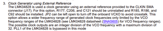
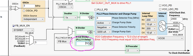
I use DAC37J84EVM board with external reference to OSCin. I did modification that is mentioned in user's guide (attached picture).

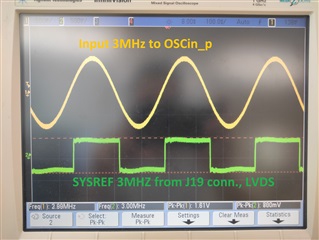
I'm using an external reference 3 MHz 2 Vpp.
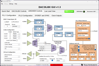
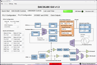
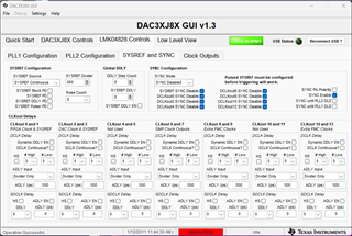
PLL2-only zero-delay with SYSREF feedback through Feedback Mux.
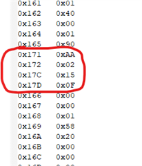
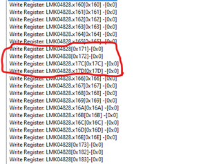
SYSREF divider = 800. Expected VCO0 frequency = 3 MHz * 800 = 2400 MHz.

When I load the configuration, usually the PLL2 doesn't lock. It locks only when I change SYSREF divider to 920 (sometimes to 812), but the VCO0 frequency becomes higher (3 MHz * 920 = 2760 MHz) than the maximum mentioned in datasheet (2630 MHz).

Why doesn't it lock with SYSREF divider = 800?
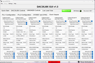
Attaching my config from DAC3XJ8X GUI.

  • Artem.

    Please send screen shots of the GUI. It takes to long to try and figure out your settings using the config file.

    Regards,

    Jim

  • Artem,

    I had trouble with this as well. I forwarded this post to our clocking team that covers the LMK device.

    Regards,

    Jim

  • Hi Jim,
    Are there any news for me?

  • Artem,

    This question is for the clock team, which I moved this post to. I will notify them to look into this.

    Regards,

    Jim

  • Hi Artem,

    The above LMK04828 config file, seems not writing all the registers and PLL2_N_CAL register doesn't contains the correct PLL2_N value, which is used for the calibration in zero delay mode.

    After making the change in PLL2_N_CAL, PLL2 will lock with 3MHz reference at OSCin.

    Below is the updated registers setting FYR.

    DAC37J84EVM_LMK04828_ZDM_e2e.txt
    R0 (INIT)	0x000090
    R0	0x000000
    R2	0x000200
    R3	0x000306
    R4	0x0004D0
    R5	0x00055B
    R6	0x000600
    R12	0x000C51
    R13	0x000D04
    R256	0x01000A
    R257	0x010155
    R258	0x010255
    R259	0x010300
    R260	0x010420
    R261	0x010500
    R262	0x0106F0
    R263	0x010711
    R264	0x010865
    R265	0x010955
    R266	0x010A55
    R267	0x010B01
    R268	0x010C20
    R269	0x010D00
    R270	0x010EF0
    R271	0x010F76
    R272	0x011008
    R273	0x011155
    R274	0x011255
    R275	0x011300
    R276	0x011400
    R277	0x011500
    R278	0x0116F9
    R279	0x011700
    R280	0x011814
    R281	0x011955
    R282	0x011A55
    R283	0x011B00
    R284	0x011C20
    R285	0x011D00
    R286	0x011EF0
    R287	0x011F11
    R288	0x012010
    R289	0x012155
    R290	0x012255
    R291	0x012300
    R292	0x012400
    R293	0x012500
    R294	0x0126F9
    R295	0x012711
    R296	0x012808
    R297	0x012955
    R298	0x012A55
    R299	0x012B00
    R300	0x012C00
    R301	0x012D00
    R302	0x012EF9
    R303	0x012F00
    R304	0x013008
    R305	0x013155
    R306	0x013255
    R307	0x013300
    R308	0x013420
    R309	0x013500
    R310	0x0136F9
    R311	0x013701
    R312	0x013800
    R313	0x013903
    R314	0x013A03
    R315	0x013B20
    R316	0x013C00
    R317	0x013D08
    R318	0x013E03
    R319	0x013F15
    R320	0x014080
    R321	0x014100
    R322	0x014208
    R323	0x014310
    R324	0x0144FF
    R325	0x014500
    R326	0x014600
    R327	0x014712
    R328	0x014802
    R329	0x014942
    R330	0x014A02
    R331	0x014B16
    R332	0x014C00
    R333	0x014D00
    R334	0x014EC0
    R335	0x014F7F
    R336	0x015003
    R337	0x015102
    R338	0x015200
    R339	0x015300
    R340	0x015478
    R341	0x015500
    R342	0x015678
    R343	0x015700
    R344	0x015896
    R345	0x015900
    R346	0x015A78
    R347	0x015BF4
    R348	0x015C20
    R349	0x015D00
    R350	0x015E00
    R351	0x015F0B
    R352	0x016000
    R353	0x016101
    R354	0x016240
    R355	0x016300
    R356	0x016401
    R357	0x016590
    R369	0x0171AA
    R370	0x017202
    R380	0x017C15
    R381	0x017D0F
    R358	0x016600
    R359	0x016700
    R360	0x016801
    R361	0x016958
    R362	0x016A20
    R363	0x016B00
    R364	0x016C00
    R365	0x016D00
    R366	0x016E13
    R371	0x017300
    R386	0x018200
    R387	0x018300
    R388	0x018400
    R389	0x018500
    R392	0x018800
    R393	0x018900
    R394	0x018A00
    R395	0x018B00
    R8189	0x1FFD00
    R8190	0x1FFE00
    R8191	0x1FFF53
    

    As you are feeding the external single ended sinewave signal as 3MHz at OSCin pin, you should apply higher amplitude signal to meet input slew rate requirement.

    Below is the graph for acceptable input range over the frequency for sinewave input.

    Thanks!

    Regards,

    Ajeet Pal

  • Hi Ajeet,
    Thanks for your answer.

    DAC38J84EVM: J25 - LMK SPI - Data converters forum - Data converters - TI E2E support forums

    According to this topic, that's not so easy to use an external LMK SPI connector to write to LMK - I need to change CPLD code.
    Could you please make a proper .cfg file that will work with DAC3Xj8X GUI, or propose the solution to write these registors to LMK on DAC37J84EVM board.

    Thanks

  • Artem,

    Use the low level view tab in the DAC38JxxEVM GUI to save your current settings to a file. Then take this file and edit the LMK section with the new values provide by Ajeet. You then can use the low level view tab to load this new update file which will then program both the LMK and DAC.

    Regards,

    Jim

  • Hi Artem,

    You can use the attached excel to convert the LMK04828 TICS Pro generated HEX config to DAC38JxxEVM GUI used config file.

     LMK04828_TICSPro_to_DAC38JxxEVMGUI_Conversion.xlsx

    Hope this will helps you.

    Thanks!

    Regards,

    Ajeet Pal

  • Hi Ajeet, thanks for the file.

    I still have problems with DAC3XJ8XGUI.
    When I load my config, it writes something else to the registers.

    Is there any easy way to write directly to LMK SPI?

    LMK_SYSREF_3M_0delay.cfg

  • Hi Artem,

    It seems the DAC GUI required to have SPACE between register and data write, where the earlier excel gives the TAB between them.

    Here is an updated conversion sheet FYR.

    LMK04828_TICSPro_to_DAC38JxxEVMGUI_Conversion_updated.xlsx 

    Thanks!

    Regards,

    Ajeet Pal

  • Hi Ajeet,
    I'm still getting the same situation, and PLL2 doesn't lock, but now N Cal Divider shows the right value of 400 (which gives total division of 800 with Prescalar = 2) after loading.

    Maybe I'll try that with dual PLL

  • Hi Artem,

    I might be suspecting the external reference (3MHz) input power. At this very low frequency, for external sine wave input it would required to have higher amplitude. You can try to validate at 15-20dBm input power.

    Anyways try with the dual PLL mode also. but this also need higher reference amplitude, when operating at 3MHz input.

    Thanks!

    Regards,

    Ajeet Pal 

  • Hi Ajeet,

    Thanks for your help. Looks like I succeeded to have PLL2 locked with these conditions:
    For ext. reference 3MHz and SYSREF 3MHz: min. sine wave ext. reference Vpp for stable PLL2 lock = 1.6Vpp;
    For ext. reference 6MHz and SYSREF 6MHz: min. sine wave ext. reference Vpp for stable PLL2 lock = 1.0Vpp.

    IMPORTANT: it locks ONLY when loading config after enabling reference clock.

    Here are working configs and waveforms.

    2816.LMK_SYSREF_3M_0delay.cfg

    LMK_SYSREF_6M_0delay.cfg

  • What I also found, that there's LMK clocks SYNC at the end of the config while pressing "Program LMK04828 and DAC3XJ8X" from Quick Start, although there's no SYNC in config saved by "Save Config".

    Here's SYNC for continuous SYSREF:

    SYNC.cfg

  • Hi Artem,

    Thanks for sharing your finding during the test and glad to know the PLL lock issue got resolved.

    Regarding the LMK clock SYNC operation, there can be various options for the SYNC, where one of them you mentioned above.

    But the internal SYNC also can be possible by setting the SYNC_PLL2_DLD bit "1" and SYNC_DISx bit "0" during the calibration. As soon as PLL2 gets lock, it generate the internal SYNC and resets the DCLK dividers and generate in-phase clocks out.

    Thanks!

    Regards,

    Ajeet Pal