This thread has been locked.

If you have a related question, please click the "Ask a related question" button in the top right corner. The newly created question will be automatically linked to this question.

ADS8588H: Max. Clock in Serial Data Read Operation

Part Number: ADS8588H

Hello,

can you please provide the updated datasheet of the ADS8588H. We need an official datasheet specifying the 50MHz SCLK frequency for timing analysis in an avionics project.

Thanks,

Matthias

  • Hi Matthias,

    We're targeting a mid-May release for an updated datasheet. Would this be acceptable?

    Best,

    -Cole

  • Hi Cole,

    if you could release the new version until May 15th, this would be sufficient. If the release is delayed, it would be very helpful if you could specify the parameters to be changed in advance.

    Regards,

    Matthias

  • Hi Mattias,

    I will talk with the team and see if they have any other comments, but this sounds like a plan for now.

    Best,

    -Cole

  • Hi Cole,
    we are going to use the ADS8588H with serial interface and OSR=0 @ 500kSps → 2µs cycle time. Could you please confirm that the following items will be considered when updating the datasheet:

    1. tCONV is too short to perform the Serial Data "Read During Conversion" of all channels with 50MHz SCLK frequency during BUSY high time only. That's why we have implemented the start of the data read before the rising edge of CONVST, so that tDZ_CSBSY is met. As a consequence, the rising edge of CONVST occurs during data read. According to chapter 7.4.1.5 the "output data can be read from the device irrespective of the status of the CONVSTA, CONVSTB pins, as there is no degradation in device performance". Please confirm, that this also applies to the rising edge of CONVST and that tD_CSCN can be ignored and will be removed from the datasheet.
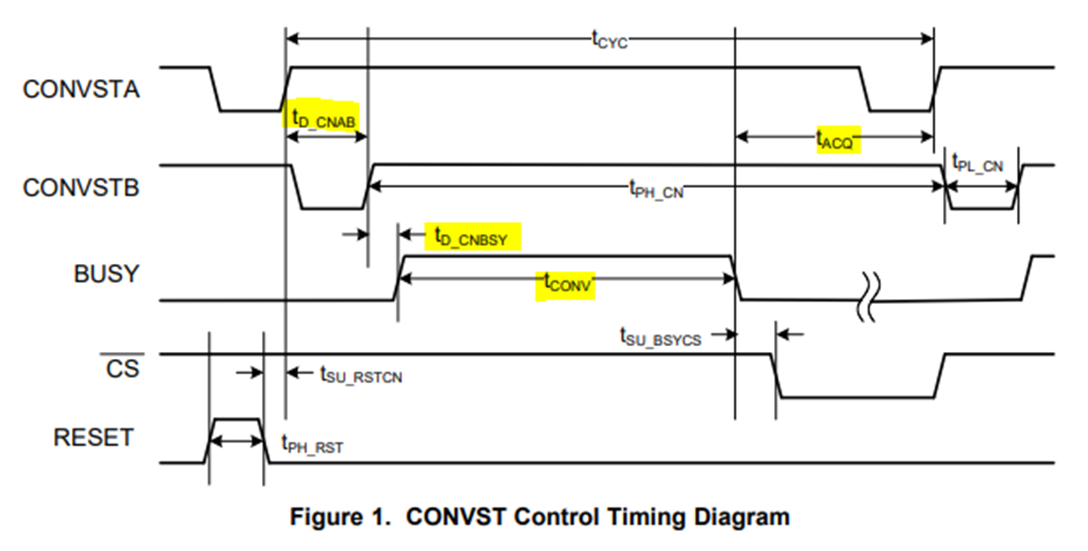
    2. When CONVSTA and CONVSTB are tied together and OSR=0 or OSR=2, the max. sum of tD_CNBSY + tCONV + tACQ is slightly higher than the 2µs cycle time. Please clarify whether tACQ is applicable when a common CONVST is used, and reduce the requested tACQ value (e.g. to 0.6µs) if applicable.
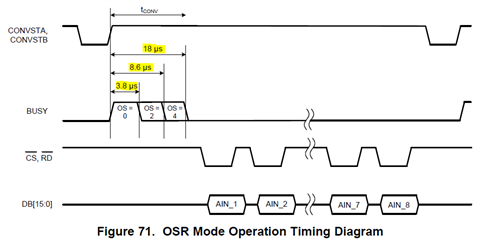
    3. Please remove or correct the BUSY high times of Figure 71.

    Regards,

    Matthias

  • Hi Matthias,

    Agreed on your analysis, I've passed the feedback to the team, we'll see what they think.

    Best,

    -Cole

  • Hi Matthias,

    We have some responses from the team.

    tCONV is too short to perform the Serial Data "Read During Conversion" of all channels with 50MHz SCLK frequency during BUSY high time only. That's why we have implemented the start of the data read before the rising edge of CONVST, so that tDZ_CSBSY is met. As a consequence, the rising edge of CONVST occurs during data read. According to chapter 7.4.1.5 the "output data can be read from the device irrespective of the status of the CONVSTA, CONVSTB pins, as there is no degradation in device performance". Please confirm, that this also applies to the rising edge of CONVST and that tD_CSCN can be ignored and will be removed from the datasheet.

    [Comments]  I am unable to visualize exactly when before the CONVST customer would start reading the data. The device surely does support reading data at any point relative to CONVST without impact on performance.

    When CONVSTA and CONVSTB are tied together and OSR=0 or OSR=2, the max. sum of tD_CNBSY + tCONV + tACQ is slightly higher than the 2µs cycle time. Please clarify whether tACQ is applicable when a common CONVST is used, and reduce the requested tACQ value (e.g. to 0.6µs) if applicable.

    [Comments] If you refer to the CONVST timing spec figure, the total cycle time is a sum of 4 specs. Among the highlighted ones below, tD_CNAB = 0 when CONVST_A/B are tied together. If I add up the max of all other specs the total time is 2.005μs. I know this is still more than the cycle time necessary for 500kHz sampling rate. However, it is important to consider that BUSY signal is an output from the ADC in response to the CONVST signal. Hence the ADC conversion begins before the BUSY signal goes high (digital output buffer delay this is usually ~5ns-10ns). Hence the acquisition time, really begins ~5ns-10ns before the BUSY signal goes low. This is not shown in the datasheet; however, this is how it would work. The CS falling edge must still follow the BUSY falling edge and not assume the 5ns-10ns output buffer delay. Short answer: tie CONVST_A/B together, clock this net at 500kHz.


    Please remove or correct the BUSY high times of Figure 71.

    [Comments]  I am not sure what is the correction expected in the BUSY high time in Figure 71. It seems as per the spec table. Please explain.

    Best,

    -Cole

  • Hi Cole,

    Thank you very much for the quick response from the team.

    1. Here is a rough diagram of the timing implemented in the driver, just for your information.

      The CONVST low pulse is generated after FRSTDATA goes low. The margin is sufficient to satisfy tDZ_CSBSY. But the tD_CSCN requirement is not fulfilled, the margin is negative. Please remove the tD_CSCN requirement from the datasheet, because according to your explanation there is no justification for requiring a "Delay between CS rising edge to CONVSTA, CONVSTB rising edge".
    2. Okay, we will connect CONVSTA/B and clock this net at 500kHz. Please confirm that reduction of the acquisition time only affects the charging of the holding capacitor (where few ns are not relevant) and not any clocked circuit that is not ready when the CONVST occurs to early.
    3. From my understanding, Figure 71 shows tCONV = 3.8µs @ OSR=0, 8.6µs @ OSR=2 and 18µs @ OSR=4. These values are outside the range given in the table in section 6.15, that you have shown in your previous answer. Did I get that wrong?

    Regards,

    Matthias

  • Hi Matthias,

    No problem. I'll pass this along to the team.

    Thanks!

    -Cole

  • Hi Matthias,

    Here is a rough diagram of the timing implemented in the driver,

    Still working on this one.

    Okay, we will connect CONVSTA/B and clock this net at 500kHz. Please confirm that reduction of the acquisition time only affects the charging of the holding capacitor (where few ns are not relevant) and not any clocked circuit that is not ready when the CONVST occurs to early.

    I've confirmed that it only affects the charging of the hold capacitor.

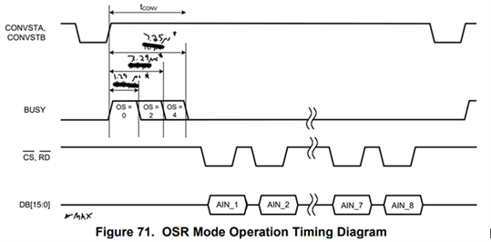
    From my understanding, Figure 71 shows tCONV = 3.8µs @ OSR=0, 8.6µs @ OSR=2 and 18µs @ OSR=4. These values are outside the range given in the table in section 6.15, that you have shown in your previous answer. Did I get that wrong?

    I've confirmed the numbers on Figure 71 are wrong and the table is correct. It should look something like this after the update:

    Best,

    -Cole

  • Hi Matthias,

    The margin is sufficient to satisfy tDZ_CSBSY. But the tD_CSCN requirement is not fulfilled, the margin is negative. Please remove the tD_CSCN requirement from the datasheet, because according to your explanation there is no justification for requiring a "Delay between CS rising edge to CONVSTA, CONVSTB rising edge".

    I actually had the same interpretation of the spec as you did, however, I wasn't reading the spec description for what it was trying to say.

    Another way to explain the tD_CSCN spec is "a CONVSTx rising edge and CS rising edge cannot be within 10ns of each other". It doesn't matter if you toggle CS high before the next CONVST, like in the figure, or if you toggle CS high after CONVST, like in your timing diagram. The 10ns is a minimum and you have almost a 1us of time between the rising edges, so you meet the spec!

    Hope that makes sense.

    Should be everything. Let me know if you have any other questions.

    Best,

    -Cole

  • Hi Cole,

    Okay. If so, please add this clarification to the datasheet. Still, it sounds strange to me. (Maybe I'm a bit confused because I cannot see a clear distinction between delay times and setup times in the datasheet. tDZ_CSBSY is called a delay time, while tSU_BSYCS is called a setup time. tDZ_CNCS and tD_CSCN are both called delay times.)
    Your answer raises the question for me whether your explanation also applies to tDZ_CNCS, due to equivalent wording in the table of para 6.7. Should the "Delay between CONVSTA, CONVSTB rising edge to CS falling edge" be understood to mean "a CS falling edge and CONVSTx rising edge cannot be within 10ns of each other"? If so, tDZ_CNCS and tD_CSCN could be combined to one timing parameter saying "a CS edge (rising or falling) and CONVSTx rising edge cannot be within 10ns of each other". So there seems to be something special about this rising edge of CONVSTx. SCLK edges are allowed in close proximity, but CS edges (rising and maybe falling) are not. Why? This is hard to understand without explanation since output registers are updated near the falling edge of BUSY.

    There is another point I would like to mention. The datasheet says "CONVSTA, CONVSTB signals can be pulled low when the internal conversion is over, as indicated by the BUSY signal (see the BUSY (Output) section)." But neither in the timing requirement tables nor in the timing diagrams is there a requirement that CONVSTx should go low only AFTER the falling edge of BUSY. On the contrary, tPH_CN is specified as 25ns min. So it seems that the text in the datasheet is too restrictive and should be adapted.

    Regards,

    Matthias

  • Hi Matthias,

    I see what you mean for the distinction between set up time and delay time. I'll see what the team says for the rest of the comments as well.

    Best,

    -Cole

  • Hi Cole,

    still waiting for the new datasheet. When will it be available?

    Regards,

    Matthias

  • Hi Matthias, 

    I saw the draft of datasheet, not sure if it was released yet. Let me check with the team.

    Thanks,

    -Cole