This thread has been locked.

If you have a related question, please click the "Ask a related question" button in the top right corner. The newly created question will be automatically linked to this question.

AMC7834: Analog and digital ground

Part Number: AMC7834

Hi Expert,

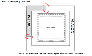
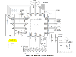
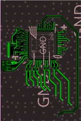
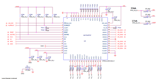
In the datasheet of AMC7834, the grounds of the analog circuit and the digital circuit are separated (first picture), but they are finally connected together at a unknown position (second picture).
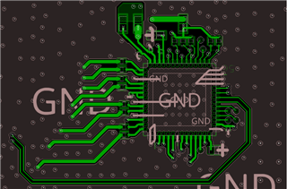
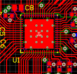
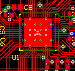
Third picture is our circuit layout, how do we achieve such a design rule?
Is there any reference layout for EVB?

Thanks,
YiTso

  • Hi YiTso,

    For the Layout Example you sent, I believe that's an example of how to place the digital and analog components, not the digital and analog ground planes. In the previous layout example, it shows the AGNDs and DGNDs routed to grounded vias. As long as your DGND and AGND are routed to the same ground plane, it will work as intended.


    Thanks,
    Erin

  • Hi Erin,

    Thanks for reply.
    Do you mean that the sample picture refers to the placement of components rather than the grounding method?
    In the actual layout,is there a limit on how far away from digital and analog pins can be grounded?
    Or just connect directly to the same ground like the sample picture through vias.
    Is there any layout or DXF file for reference?

    Thanks,
    YiTso

  • Hi Erin

    Btw, can you help review this layout about ground connection?
    Schematic shown in the screenshot.

    Thanks,
    YiTso

  • Hi YiTso,

    Yes, I mean that the reference picture in your initial question is for the placements of analog/digital components, not the expected grounding method. For the layout, ideally you would want the AGND/DGND to be grounded close to the DUT. I've attached an image of our EVM layout showing the grounded vias, which happen to be the four vias closest to the DUT. 

    Your layout grounding looks good. It appears that everything is grounded close to the DUT, which is what TI recommends. I don't believe you'll have any issues with grounding.


  • Hi Erin

    Thanks for your reply.
    Another question is why only the DGND pin seems to be connected to the thermal pad in the middle, but AGND doesn't use this method?

    Thanks,
    YiTso

  • Hi YiTso,

    In this case, the evaluation board set the thermal pad to VSS, since we use both negative and positive ranges for the board. Pin one is on the bottom left, so the pin you circled is VSS. I'm not entirely sure why it was decided to connect the VSS pin to the pad (they may have not had a VSS plane for the vias so they needed a trace connection), but a connection to the thermal pad is not necessarily required if it is grounded. Let me know if you have any other questions.

    Thanks,
    Erin

  • Hi Erin,

    Thanks for the further explanations. 

    Regards,

    YiTso