This thread has been locked.

If you have a related question, please click the "Ask a related question" button in the top right corner. The newly created question will be automatically linked to this question.

ADC121C021: Rare I2C lockup problem

Part Number: ADC121C021
Other Parts Discussed in Thread: TPS22917

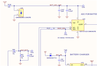
We are using the ADC12C021 similar to that shown in "ADC121C021: Oddly sensitive to value of capacitor on VIN" but with the battery voltage taken directly from the "HALF_BATT" location rather than after a buffer / amp.  

We have a problem in that sometimes when we first apply external power to our unit (including the ADC121C021), the chip doesn't respond to I2C commands; I suspect it's not getting an "Acknowledge" bit but I haven't been able to confirm that yet.  Repeated attempts to read the I2C bus continually fail until we power the unit down and back up again, at which point it works perfectly.  No other devices on the same I2C bus exhibit this problem. 

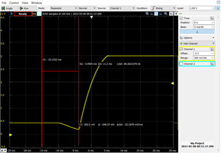
We suspect that the issue has something to do with the fact that there is still a small current (< 25uA) coming through VIN from the battery when the device is powered down.  This can leave a residual voltage on VA (the chip's power pin) of about 450mV, which takes a dip down to 200mV just after external power is reapplied (see scope image below).  The datasheet indicates "The internal registers will lose their contents if the supply voltage goes below 2.4V.  Should this happen, it is important that the VA supply be lowered to a maximum of 200mV before the supply is raised again to properly reset the device and ensure that the ADC performs as specified."  

If we don't leave the unit off long, we don't always go below 200mV as shown in the plot, but I have never seen the chip fail an I2C access when I've scoped it up like this.  However, if I let the unit sit overnight with power off, and battery current slowly leaking through the dividers and the chip - perhaps draining fully - on (only) the very first power-up in the morning, I2C accesses for this chip fail.  All other power-ups throughout the day are fine.  

Unfortunately, this chip doesn't have an external reset pin, so we can't force it to a known state if the I2C bus locks up.  Fortunately it doesn't affect other devices on the bus when this happens.  This failure has been very hard to reproduce in the lab, but it comes up often enough on the production floor to delay testing / deliveries.  I have tried reproducing the problem by letting the battery drain 1 to 5 hours, but it seems to require an overnight duration for it to show up.

To meet the full datasheet requirements, it looks like we will need a circuit to disconnect the battery when power is off to avoid this problem, but we haven't tested that yet as that would require major board changes.  Can we avoid this problem by increasing the battery divider resistors to some minimum level?  Can you give us any insights in how to mitigate this issue?  

Thanks,

Cynthia

  • Hi Cynthia,

    Thank you for your question! Could you please share your schematic so we have a better understanding of the issue?

    Best,

    Samiha

  • The schematic is very similar to that shown in "ADC121C021: Oddly sensitive to value of capacitor on VIN" (which this question is related to) but the "HALF_BATT" signal goes directly to VIN on the chip, rather than through the amp & RC filter shown there.  

  • It would help to see what the circuit looks like leading up to VA and VIN. Thanks!

  • From what you are describing, it sounds like your issue may have to do with the analog power supply VA, whereas in the E2E post you tagged, it sounds like they are describing a problem with VIN. It would help to see your schematic and what the analog supply circuit looks like.

    Also, when the device is powered down, are you still applying a voltage to VIN?

  • Yes, Scott is describing a different problem there, but my schematic is almost the same except for the difference note above.  I've included the image here so you can confirm that.  And yes, the battery voltage (from a single LiFePO cell) attaches to the resistor network on the left side of R60, and is still there when the device is powered down, i.e. when the +3.3V supply into the regulator (in the northwest corner) goes away.

  • Thanks for sharing your schematic! To meet datasheet requirements, an option that may work is using a load switch like TPS22917 to turn off VIN when the device is powered down. You could connect your battery (before or after the resistor divider) to pin 1 of TPS22917, your analog supply to pin 3, and ADC VIN to pin 6.

  • Could our current situation explain a lock-up of the IC, though?  We can certainly come up with fixes which involve a schematic change, but we're trying to understand the current problem in order to determine the urgency of the design change.  We're already shipping product.

    Thanks,

    Scott

  • Hi Scott, the current situation could explain why the IC is not behaving as expected. For normal operation, the IC is expecting VIN to be between 0V and VA.

  • Hi Samiha,

    The TPS22917 currently available at Digi-Key is 22.5 cents each (3k qty).  If making sure VIN has no current when power if off is the issue, then the complementary FETs in an FDY4001CZ (10 cents each at 2885 qty) and a pull-up resistor could do that for me at about half the cost.  

    However, I'm not 100% sure this is causing the lock-up problem though, as Scott has asked.  Given that it is a difficult problem to replicate in the lab, we were hoping you had more definitive and quantitative information on whether or not this leakage current when the device is off for long periods could really be the problem.

    As I mentioned in my first message, I have seen the 200mV "OFF" voltage violated numerous times and the part didn't fail when I brought it back up, so I'm not quite sure if cutting off the battery is going to fix it.  If there are other things that could cause this that you know of, I'd like to check them on my system.

    Thanks for your help,

    Cynthia

  • Hi Cynthia,

    I understand your point that it does not always fail when the "off" voltage is violated, that is interesting. My understanding is that outside the normal operating range (like when VIN is not between 0V and VA), the device behavior may be unexpected, which is hard to quantify. The device may be damaged, and thus fail, when the absolute maximum ratings are surpassed, which doesn't seem to be an issue in the attached schematic. Let me do some further reading and check with my team to see if I can find any more information. I will get back to you by tomorrow at the latest. Thank you!

    Best,

    Samiha

  • Hi Cynthia,

    There doesn't seem to be any more helpful information regarding this issue that I could find. I am curious though - did you and Scott experience a similar I2C lockup when including the buffer/amplifier in your circuit?

  • The revision with the buffer was a short-lived prototype due to the oscillation problem.  This really didn't become an issue for us until we built around 300 of them and about 10% failed the first time through the assembly test procedure.  So far, I can still only produce it once on some boards on the first power-up in the morning.  The rest of the day it works fine, whether I have partially, hardly, or fully discharged the battery.

    At this point, given the difficulty in reproducing it, I'm concerned about making board level changes because I'm not sure if I'll actually be addressing the root cause of the problem.

    Thanks for your help.