This thread has been locked.

If you have a related question, please click the "Ask a related question" button in the top right corner. The newly created question will be automatically linked to this question.

ADC32J25: Interfacing with FPGA

Part Number: ADC32J25
Other Parts Discussed in Thread: LMK04828, , ADC32J24

Hello,

Now we have the board, and the board has been verified including the clock generation with LMK04828 and FPGA

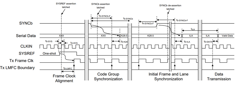
We are now trying to get the JESD204B working between ADC32J25 and FPGA.  

We are leveraging a previously working FPGA design with JESD204B.

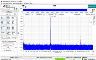
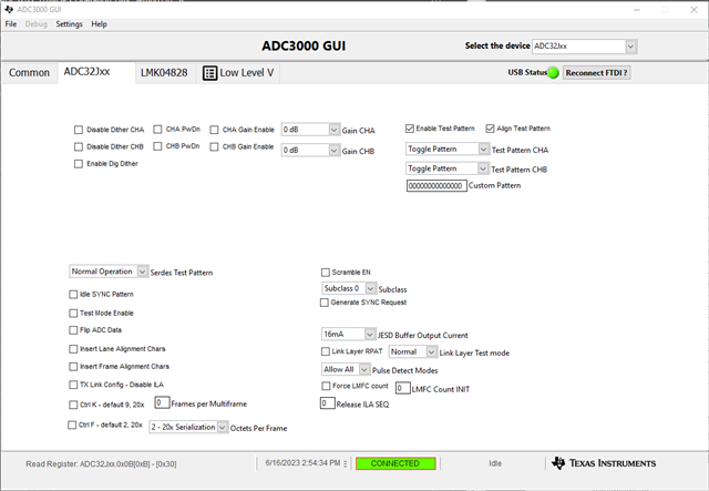
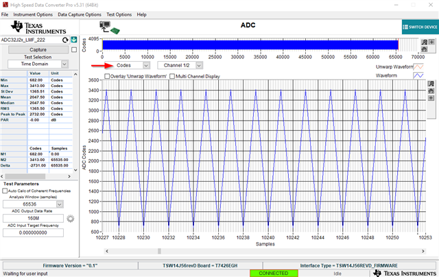
The 1st step is to see if we can receive a test pattern from ADC32J25.

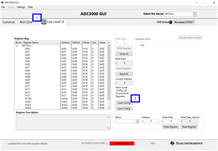
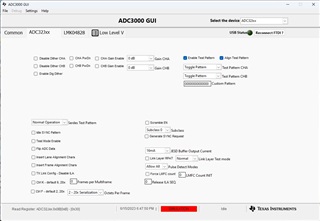
Attached is the ADC register configuration.

Would you be able to take a look at the configuration?

Regards,

Andrew

00400100
00400300
00400400
00400602
00400700
00400800
00400900
00400A03
00400B30
00400C00
00400D00
00400E00
00400F00
00401300
00401500
00402700
00402A56
00402B01
00402F00
00403001
00403114
00403420
00403A00
00403B40
00403C00
00442200
00443400
00452200
00453400

  • Hello Andrew,

    I'm not sure what exactly you would like for me to check from your configuration. When I loaded it to the GUI, I was able to obtain a capture, meaning the ADC is outputting data (picture below where I have my analog input operating at 25-MHz and 10dBm).

    Also, 5516.ADC3xJxx_128MSPS_Operation_LMK_Setting.cfg is the default config file in case that's what you were looking for. You can load it by clicking on the "Low Level Vi" tab, and then the "Load Config" button.

    If you could also write you set up the GUI to do, that would be very helpful as well.

    Thanks,

    Andrea

  • Hi Andrea,

    Thanks for your help.

    I set up the configuration to generate the test pattern (K.25) as opposed to capturing the ADC data.

    I've noticed in the ADC3000 GUI screencapture, it looks like all the registers are set to zeros.

    So for normal ADC operation, the defaults are all zeros.  Is this correct?

    I can format my config file so you can load it.

    I have a question on the format.

    If you look at the format I used (intended to load into our FPGA)

    For example, 

    00400602

    • the leading two "0"s are fill bits
    • "40" indicates I'm writing to the ADC
    • "006" is the register address
    • "02" is the register value

    Could you see if the format would work?

    Let me also write you on the clock architecture.  

    But I just wanted to see if the data format I used is consistent.

    Regards,

    Andrew

  • Hi Andrea,

    We are following the write format described on pg 55 of the datasheet

    So the "0" corresponds to the fact that A14 should be "1".

    Thank you,

    Andrew

  • config_fpga1.cfg

    I've reformatted the config file so you should be able to load into the GUI.

    I also noticed in ADC3000 GUI 

    • If I select ADC32Jxx, both LMK04828 and ADCJxx show up
    • If I select ADC32xx, only ADC32xx shows up

    I am assuming either one is okay.

    Thanks again,

    Andrew

  • Hello Andrew,

    So for normal ADC operation, the defaults are all zeros.  Is this correct?

    Correct, the default for all registers for the ADC32J24 are 0x00.

    Could you see if the format would work?

    Looking at the last config file you uploaded, that should be able to work IF you change line 1 from "ADC32xx" to "ADC32Jxx" and use the ADC32Jxx GUI page. If not, the data won't be read into the GUI. Also, it looks like in line 12 you did not finish writing that register write. Default_ADC32Jxx.cfg is the file from the default GUI for the ADC32Jxx page.

    I am assuming either one is okay.

    When I loaded the file yesterday to the GUI, I accidentally used the ADC32xx GUI page; however, we recommend to use the ADC32Jxx GUI page instead for this part. All the tests that I ran today to answer your questions where with the ADC32Jxx GUI page.

    I believe I have answered all your questions, if not, please do let me know or if you have any further questions.

    Good Luck,

    Andrea

  •  config_fpga2.cfg

    Hi Andrea,

    We are still troubleshooting.  

    In order to have a better visibility, we would like to see if we can detect a test pattern.

    Could you take a look at the screenshot and see if the test pattern generation is configured correctly?

    Also included is the config file.  Would it be possible for you to load the config file into your setup for verification?

    Thank you for support.

    Andrew

  • Hello Andrew,

    Could you take a look at the screenshot and see if the test pattern generation is configured correctly?

    By just looking at the screenshot, the GUI should be setup correctly for that page. I set my GUI up the same way for that page and I obtained a capture showing the pattern toggling (from the Codes window; however, from the Real FFT window I saw nothing):

    Here is my config with a working system (both LMK04828 and ADC32J25).

    TestPattern_Toggle_ADC32J25.cfg

    Also included is the config file.  Would it be possible for you to load the config file into your setup for verification?

    When I loaded the config file into my setup, the ADC was not picking up a clock, and hence, I was not able to obtain a capture. This means your configuration for the LMK04828 is incorrect since the part is not able to lock the PLL (when LED D4 is lit, it means the LMK04828 PLL is locked). If you tell me what frequencies you would like to output, if you have a set input frequency, and if there are any other requirements (such as SYSREF, etc) that you need from the LMK04828, I can help create a config with the correct LMK04828 setup.

    Also, note that you don't need to check the "Align Test Pattern" option to output a test pattern. You only need to check that box if you need to align the outputs of the test patterns across the different channels. Hope this helps and let me know if you need anything else from me.

    Good Luck,

    Andrea

  • Hi Andrea,

    I thank you so much for your support.

    I think we are getting close to figuring out the root cause, something related to clocks.

    Just realized the sampling clocks and SYSREF signals were set to LVDS but the circuit design is intended for LVPECL.

    I set the signal type to LVPECL20 now.

    Here are the TICS Pro files

    LMK04828b_v061623a.tcs

    R0 (INIT)	0x000090
    R0	0x000010
    R2	0x000200
    R3	0x000306
    R4	0x0004D0
    R5	0x00055B
    R6	0x000600
    R12	0x000C51
    R13	0x000D04
    R256	0x01000F
    R257	0x010155
    R258	0x010255
    R259	0x010301
    R260	0x010402
    R261	0x010500
    R262	0x010670
    R263	0x010711
    R264	0x01080F
    R265	0x010955
    R266	0x010A55
    R267	0x010B00
    R268	0x010C22
    R269	0x010D00
    R270	0x010E70
    R271	0x010F66
    R272	0x011018
    R273	0x011155
    R274	0x011255
    R275	0x011300
    R276	0x011402
    R277	0x011500
    R278	0x0116F0
    R279	0x011711
    R280	0x011818
    R281	0x011955
    R282	0x011A55
    R283	0x011B00
    R284	0x011C02
    R285	0x011D00
    R286	0x011EF1
    R287	0x011F17
    R288	0x012018
    R289	0x012155
    R290	0x012255
    R291	0x012300
    R292	0x012402
    R293	0x012500
    R294	0x0126F1
    R295	0x012711
    R296	0x012808
    R297	0x012955
    R298	0x012A55
    R299	0x012B00
    R300	0x012C02
    R301	0x012D00
    R302	0x012EF9
    R303	0x012F00
    R304	0x013018
    R305	0x013155
    R306	0x013255
    R307	0x013300
    R308	0x013402
    R309	0x013500
    R310	0x0136F1
    R311	0x013766
    R312	0x013800
    R313	0x013900
    R314	0x013A01
    R315	0x013B2C
    R316	0x013C00
    R317	0x013D08
    R318	0x013E03
    R319	0x013F00
    R320	0x01400B
    R321	0x014101
    R322	0x014200
    R323	0x014319
    R324	0x014400
    R325	0x01457F
    R326	0x014600
    R327	0x01471A
    R328	0x014802
    R329	0x014942
    R330	0x014A02
    R331	0x014B16
    R332	0x014C00
    R333	0x014D00
    R334	0x014EC0
    R335	0x014F7F
    R336	0x015003
    R337	0x015102
    R338	0x015200
    R339	0x015300
    R340	0x015478
    R341	0x015500
    R342	0x015664
    R343	0x015700
    R344	0x015896
    R345	0x015900
    R346	0x015A64
    R347	0x015BD4
    R348	0x015C20
    R349	0x015D00
    R350	0x015E00
    R351	0x015F0B
    R352	0x016000
    R353	0x016101
    R354	0x016225
    R355	0x016300
    R356	0x016400
    R357	0x01650F
    R369	0x0171AA
    R370	0x017202
    R380	0x017C15
    R381	0x017D33
    R358	0x016600
    R359	0x016700
    R360	0x01680F
    R361	0x016959
    R362	0x016A20
    R363	0x016B00
    R364	0x016C00
    R365	0x016D00
    R366	0x016E13
    R371	0x017300
    R386	0x018200
    R387	0x018300
    R388	0x018400
    R389	0x018500
    R392	0x018800
    R393	0x018900
    R394	0x018A00
    R395	0x018B00
    R8189	0x1FFD00
    R8190	0x1FFE00
    R8191	0x1FFF53
    

    Also in terms of SYNCP/N signals, they are designed as straight CMOS.  So there is no 100 Ohm resistor between the P/N traces.

    3755.fibersense_v1p23.pdf

    • Sheet 2: FPGA pins for ADC32J25
    • Sheet 15: ADC32J25
    • Sheet 18: LMK02828B

    Would it be an issue for SYNCP/N not to have a 100 Ohm resistor in between?  

    Looking at the table in Section 7.12 of the ADC32J25 datasheet, VIH = 1.3 and VIL = 0.5.

    So perhaps the design may still work.  Otherwise some rework may be needed.

    Appreciate your support.

    Thank you,

    Andrew

  • Hello Andrew,

    Here are the TICS Pro files

    I'm working on converting and loading the .tcs file to the ADC GUI, so I'll get back to you by early next week with an answer. In the meantime, are you using PLL1 at all? All your CLKinXs are disabled so no signal will get through to PLL1 even if it's powered up.

    Would it be an issue for SYNCP/N not to have a 100 Ohm resistor in between?  

    It is not an issue as long as FPGA pin for this diff pair has a 100-Ω internal termination.

    Best,

    Andrea

  • Hi Andrea,

    Thanks for the update.

    We have verified the LMK048288 is working again (not certain anything in the FPGA or just some mistake in LMK04828 registers).

    We have also verified that the FPGA can take LVDS (without 100 ohm) from LMK04828.

    Now with the FPGA working again I think if you can share ADC GUI settings I can try to figure out how to translate to TICS Pro settings.

    Regards,

    Andrew

  • Hello Andrew,

    I am glad you got the LMK04828 to work and provide a sampling clock to the ADC.

    What do you mean by ADC GUI settings? Above I attached the test pattern you requested to ensure you were able to communicate with the ADC (here is it attached again: TestPattern_Toggle_ADC32J25 (1).cfg). However, for me to create a config, I need to know at what frequency you're sampling (which I believe is 160-MHz from your schematic) and what exactly you need from the ADC. Then, I can generate a file for you and send it over. Once I get more clarification I can better support you.

    Best,

    Andrea

  • Hi Andrea,

    Sorry for delay.  I was able to spend some time and here is where things stand.

    1. I have gotten familiar with the ADC registers
      1. First I tried various combinations of 2Ah (SERDES Test)
      2. I believe this control the patterns at the JESD level so any ADC data will be ignored
      3. I see bcbc... which I believe is K28.5 characters
      4. They are fairly consistent.  Does it mean that most of the clocks are working?
      5. However, I try to send test ADC pattern as you also suggested in the ADC config file, 010101...
      6. But I'm still seeing bcbcbc...
    2. The ADC sampling clock is 160 MHz and the SYSREF is 8 MHz
      1. My LMK04828 configuration is a bit different because I use it to generate various clocks.
      2. However, I have verified I can control the LMK04828.  

    I'm also attaching the schematic.  A couple of things I would like to ask

    1. From the ADC datasheet, the ADC outputs (DAP/M, DBP/M) are CML.
    2. In our schematic they are treated as LVDS with the internal 100 Ohm termination within the FPGA
    3. Hope this is equivalent
    4. As for SYNCP/M~, the FPGA provide 3.3 CMOS signals.  In fact, I am not certain it is possible to generate LVDS from the regular IOs on the FPGA (Xilinx Kintex7)

    At this point, I think everything should be correctly set up:

    1. LMFS = 2221 and K=8
    2. Btw I think there is a typo in the ADC datasheet.  In Table 29. Register 2Bh Field Descriptions, 0 = Default is 9 (I think it should be 8)
    3. Also in 30h and 31h, they use a zero offset, meaning if K=8, Register 31h should be set to 0x07 (not 0x08).

    Attached below are

    1. screen captures of the Vivado ILA
    2. Schematic (ADC is on Sheet 15, JESD on FPGA is on Sheet 5, ADC config control is on Sheet 2
    3. ADC config used

    I sincerely appreciate your support.

    Regards,

    Andrew

    fpga_captures_070123.pptx

    3808.fibersense_v1p23.pdf

    00C00600
    00400601
    00C00600
    00400100
    00400300
    00400400
    00400602
    00400700
    00400800
    00400902
    00400A03
    00400B20
    00400C00
    00400D00
    00400E00
    00400F00
    00401300
    00401500
    00402700
    00402A00
    00402B03
    00402F00
    00403001
    00403107
    00403420
    00403A00
    00403B00
    00403C00
    00442200
    00443400
    00452200
    00453400
    00C00100
    00C00300
    00C00400
    00C00600
    00C00700
    00C00800
    00C00900
    00C00A00
    00C00B00
    00C00C00
    00C00D00
    00C00E00
    00C00F00
    00C01300
    00C01500
    00C02700
    00C02A00
    00C02B00
    00C02F00
    00C03000
    00C03100
    00C03400
    00C03A00
    00C03B00
    00C03C00
    00C42200
    00C43400
    00C52200
    00C53400
    

  • I just tried the same ADC settings you provided, and just triggered on the rx_tdata (received data in FPGA via JESD).

    The data looks like: 54aa54aa5455a01c

    Is this something close what was expected?

    I understand the test pattern was: 1010...0101...

    Perhaps we may be missing some bits but hopefully it means we are getting closer.

    Thanks again,

    Regards,

    Andrew

    fpga_captures_070123a.pptx

  • Hello Andrew,

    I will get back to you at the end of the week once I get back to the office after the holiday weekend in the US.

    Best,

    Andrea

  • Andrew,

    0xBCBC indeed refers to K28.5 characters and shows that the ADC is in CGS stage of bring-up sequence. See below image. 

    Can you add SYNC to the ILA IP block and also trigger your ILA on SYNC de-assertion (rising edge of SYNC) and verify that data changes from 0xBCBC to K28.0 character and Dx.y data symbols? 4 multi-frames after the SYNC de-assertion the actual ADC data will be present at the FPGA if the ADC has exited ILAS (initial lane alignment sequence).

    What is the rx_tvalid signal in your ILA?  

    Thanks, Chase

  • HI Chase,

    Let me work on this (again sorry for delay due to my traveling).

    Thank you,

    Andrew