A related question is a question created from another question. When the related question is created, it will be automatically linked to the original question.
If you have a related question, please click the "Ask a related question" button in the top right corner. The newly created question will be automatically linked to this question.
I am trying to use an Arduino MEGA and the SPI protocol to control the DAC outputs. I have all of the power inputs correctly powered according to the test points so I suspect my issues lie in my program.
The goal of the program in its current iteration is to power on the DAC outputs at 5V on command from the board.
I suspect that the issue lies in differential mode. I do not understand what steps must be taken with the registers and jumpers to allow me to achieve my goal, which I believe means disabling differential mode.
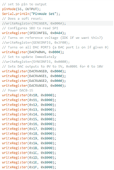
The program I have written is described below, although the definitions of all of the registers is not included (though declared in the environment).
voidsetup(){
Serial.begin(9600);
Serial.println("Setup");
// put your setup code here, to run once:
SPI.begin();
SPI.setBitOrder(MSBFIRST);
SPI.setClockDivider(SPI_CLOCK_DIV4); // 4MHz
SPI.setDataMode(SPI_MODE1); // CPOL = 0, CPHA = 1
// set SS pin to output
pinMode(SS, OUTPUT);
Serial.println("Pinmode Set");
// Configures SDO to read SPI
writeRegister(SPICONFIG, 0x0004);
// Turns on reference voltage (IDK if we want this?)
writeRegister(GENCONFIG, 0x3F00);
// Turns on all DAC PORTS (a DAC port is on if given 0)
writeRegister(DACPWDWN, 0x0000);
// Set to update Immediately
writeRegister(SYNCONFIG, 0x0000);
// Sets DAC outputs to 0V to 5V, 0x0001 for 0 to 10V
writeRegister(DACRANGE0, 0x0000);
writeRegister(DACRANGE1, 0x0000);
writeRegister(DACRANGE2, 0x0000);
writeRegister(DACRANGE3, 0x0000);
Serial.println("Setup Done");
}
voidloop(){
// Register adresses are 8 bits
// Registers store 16 Bits
Serial.println("Start");
//Writes to DAC ports
writeRegister(DAC0, 0x8000);
writeRegister(DAC1, 0x8000);
writeRegister(DAC2, 0x8000);
writeRegister(DAC3, 0x8000);
writeRegister(DAC4, 0x8000);
writeRegister(DAC5, 0x8000);
writeRegister(DAC6, 0x8000);
writeRegister(DAC7, 0x8000);
writeRegister(DAC8, 0x8000);
writeRegister(DAC9, 0x8000);
writeRegister(DAC10, 0x8000);
writeRegister(DAC11, 0x8000);
writeRegister(DAC12, 0x8000);
writeRegister(DAC13, 0x8000);
writeRegister(DAC14, 0x8000);
writeRegister(DAC15, 0x8000);
Serial.println("Casting");
delay(1000000000);
}
// Transfers 16 bit (4 hex digit) value to the register given
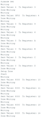
This is the output (minus some more of the writes to the pins as seen at the bottom) when I run that script, but I plan to check with an oscilliscope to see if these commands are actually being sent.
In the meantime, can you share a screenshot of one of your write commands. It is helpful for us to verify that the timings are being met. Also, are you using the DAC81416EVM or another board? If it is the EVM, please share all of the jumper settings. If it is another board, can you please share the schematic.
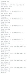
This image results from the "writeRegister(DAC10, 0x8000);" call.
The writeRegister function I wrote has been modified to print out the value received from the transfer of the value to the address, with the new code given below:
// Transfers 16 bit (4 hex digit) value to the register given
voidwriteRegister(byte address, unsignedintval){
Serial.println("Writing");
digitalWrite(SS, LOW);
//SPI.beginTransaction(settings);
SPI.transfer(address);
uint16_t x = SPI.transfer16(val);
//SPI.endTransaction();
Serial.print("Sent Value: ");
Serial.print(val, HEX);
Serial.print(" To Register: ");
Serial.println(address, HEX);
Serial.print("Got Value: ");
Serial.println(x, HEX);
// add delay?
digitalWrite(SS, HIGH);
Serial.println("Done Writing");
}
The jumpers are currently in the following positions:
J2: open
J3: open
J9: open (REFGND connected to GND on the power supply for VCC, VAA, & VIO; confirmed by the GND test points)
J10: 2-3 (providing 5V as VIO to J7.4; confirmed by VIO TP)
J11: 1-2 (REF5025) (This is the one I feel unsure about)
The code to write 0x8000 to each of the DAC registers returns 0x0000 for some of the registers in the loop while returning 0x8000 for a minority of the registers. The value returned by the DAC register appears to be randomly selected from these two, at least to me.
I ran the left picture, producing the right picture. I monitored the SPI signals sent with an Oscilloscope and they are definitely being sent by the board.
I still receive no voltage drop between any of the output pins of the DAC & GND.
Assuming by digital test point you meant VDD, I have the following oscilliscope trace. It may be hard to tell, but it is at 5V (the top line) compared to (1) the green square below it (confirmed by multimeter)
1. why ch2 (SCL) in both plots have voltage levels ~0.35V only? please make sure that digital line (SCL, SDI and SYNC) have voltages as per VIO supply.
2. I am not able to understand the MOSI data from the plot, please capture a full pattern frame and verify if the MOSI data is matching with scope capture.
3. SCL is not clean, please reduce the speed ~ 100KHz instead of 4MHz.


 This is the output (minus some more of the writes to the pins as seen at the bottom) when I run that script, but I plan to check with an oscilliscope to see if these commands are actually being sent.

 MISO (TOP), SCK (BOTTOM)
 MOSI (TOP), SCK (BOTTOM)