This thread has been locked.
If you have a related question, please click the "Ask a related question" button in the top right corner. The newly created question will be automatically linked to this question.
Hi TI Expert,
I need to design a optical detector with wide dynamitc range so the input voltage to the AIN_P may be very large, for instance 3.4V.
And I notice that when the AIN_P is large and clamped by the the ADC's internel diode (clamped to around 2.3V), there will be a signal around 3mV crosstalk detected by the channel B (read from ADC).
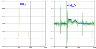
1) I tried adding external diode 1SS315TPH3F connected to the 1.8V power of ADC,now the it's clamped to around 2V, but still the crosstalk can be detected.
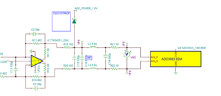
2) I tried limited the voltage to around 1.5V by connected the diode to a voltage devider.
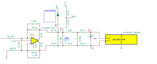
Now the crosstalk seems disapeared.
I guess no one can guarantee the reliablity/crosstalk when the ADC gets overvoltage stress even if it only lasts 50~100us regularly, so the clamp is needed.
My concern is the diode's forward voltage is not constant and adds extra capacitor (Although my application is a low frequency one (<1MHz)), and I'm not sure if it distort the signal.
Is is OK or is there any other solution more reasonable?
Thanks!
Hi Follin,
Why is there a diode only on one side of the differential inputs?
That might be the issue.
These types of things are best measured on the board, layout can play a big part in crosstalk measurements and deviate away from any simulation.
Regards,
Rob
Hi Rob,
The simulation circuit pic is only to show the circuit and solution, I did the test on the board and read the adc data.
The overvoltage only happened at the AIN_P so currently I only added the diode on it and then the crosstalk disapeared. It is solution (2) talked above.
In the waveform you may see the crosstalk only happens when the FDA output is saturated (flat top), and after the AIN_P is clamped to 1.5V the crosstalk disapears. If it's caused by the layout only, the crosstalk at channel B should get large at the moment of the rising and falling edge of the pulse at channel A.
I've multiple ADC3683 on the board, and in this experiment, the crosstalk only happens between two channels of one chip.
Hi Follin,
You are correct in that we cannot guarantee crosstalk performance when the ADC is overdriven as this behavior will change from each device. Anything beyond the datasheet max operating conditions and TI cannot guarantee the device will function. Anything beyond the recommended operating conditions table in the datasheet and TI cannot guarantee the performance will match the datasheet metrics.
There should be the same clamp on the negative input as well to avoid an unbalanced input network when the negative pair swings positive. Regarding your adjustable level clamp, it makes sense that anything above 2.1V is likely to cause strange performance in the device as we cannot guarantee functionality when the input is above 2.1V. And it also makes sense that at 1.5V, the crosstalk will seemingly disappear (to the datasheet listed spec), as the input is clamped to an appropriate level (less than full scale). I suggest you implement this clamp design on all of your FDA outputs.
Regards, Chase