This thread has been locked.

If you have a related question, please click the "Ask a related question" button in the top right corner. The newly created question will be automatically linked to this question.

AFE7070EVM: GUI Controls for Mixer/NCO & More

Part Number: AFE7070EVM

We are using the AFE7070EVM standalone (no TSW1400).

The mixer/NCO is enabled and GUI settings are as shown below. The CMCD7005 is in default state = bypass mode.

LO Input = 2.2 GHz. from signal generator
EXT VCXO Input (J4) = 65 MHz 0 dBm from signal generator


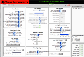
This produces an output spectrum like this which appears to be a lower sideband tone offset by the NCO frequency setting value (1 MHz):

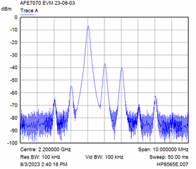
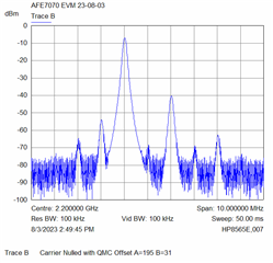
Enabling QMC offset and manually playing with the QMC A & B Offsets the carrier can be nulled = good.
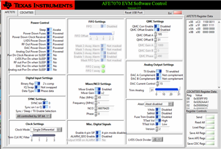
Questions:

1) What is the proper GUI lower left "Clock Settings" when using the EVM this way? It is currently set to single differential SDR clock and with the NCO Fdac setting matching the VCXO input frequency, the output tone is 1 MHz away from the carrier, which matches the GUI NCO Frequency setting. What is Clock settings changing and/or what is the relationship between clock settings and the transmitted result?

2) Enabling QMC Correction and playing with the QMC gain so far only produces worse rejection of the upper sideband. How should adjustments be made to optimize this? Or in other words, what is the procedure to set up an optimized single sideband output and an optimized double sideband output?

3) Are there any other controls that should be adjusted when using the AFE7070 EVM for basic TX output tests?

  • LL: Please see my responses below.  --RJH

    1) What is the proper GUI lower left "Clock Settings" when using the EVM this way? It is currently set to single differential SDR clock and with the NCO Fdac setting matching the VCXO input frequency, the output tone is 1 MHz away from the carrier, which matches the GUI NCO Frequency setting. What is Clock settings changing and/or what is the relationship between clock settings and the transmitted result?

    RJH>> The clock modes options are described in the datasheet on page 27.  I usually operate in Dual Output Clock Mode and inject a 2x clock frequency (130 MHz in your case) to the EVM.  You still specify the NCO sample clock (Fdac) at 65 MSPS.

    2) Enabling QMC Correction and playing with the QMC gain so far only produces worse rejection of the upper sideband. How should adjustments be made to optimize this? Or in other words, what is the procedure to set up an optimized single sideband output and an optimized double sideband output?

    RJH>> Optimization of the unwanted sideband requires balancing the gain and phase of the input BB paths.  The primary adjustment will be with the phase with only a minor tweak to the gain.  Start off with the the gain settings at 1024 for both Gain A and B and Phase at 0.  From there, start with tweaking the phase to get improvement.  This value can go positive or negative.  Once that is optimized, you can tweak the gain on just on the gain paths.  You should only have to adjust this by a maximum of only 1 to 3 steps.  Then you can iterate that process with adjusting the phase and tweaking the gain to get the best optimized performance.

    3) Are there any other controls that should be adjusted when using the AFE7070 EVM for basic TX output tests?

    RJH>> You can adjust the DAC Current Control as a way to adjust output power.  Settings in the 10 - 15 range are typical.  You can also adjust the programmable filter setting with the Trim Analog setting.  As mentioned before, the QMC Gain setting nominal setting is 1024.  Adjusting A/B controls in unison facilitate a digital gain control.