This thread has been locked.

If you have a related question, please click the "Ask a related question" button in the top right corner. The newly created question will be automatically linked to this question.

DAC3154: Schematics for DAC3154

Part Number: DAC3154
Other Parts Discussed in Thread: DAC3152, , TRF370417, DAC3174, TRF3705

Unfortunately I couldn't find any schematics from DAC31x1 nor DAC31x4 (these would be pin compatible). Also the EVM board doesn't have any schematic with it. I would appreciate it, if you would send me these along with the layout of your design, so I can orient myself on the the constraints. The datasheets are missing some informations, that I would like to clarify here:

1. The DACCLK is LVPECL (for that the Common-mode voltage is 2V, but in the datasheet it's mentioned as 0.5V?), but in another datasheet (DAC3152 page 17/32) you mentioned that the DACCLK pins are internally biased and "Although not optimal due to the limited signal swing, an LVDS source can also be used to drive the clock input", but I'm not sure, if this applies to the DAC3154? The LVDS has VDIFF of 400mV, so it's barely the minimum of what DACCLK could take. Is this a reliable clock configuration? Only AC coupling won't do much, but your internal biasing is maybe helpful?
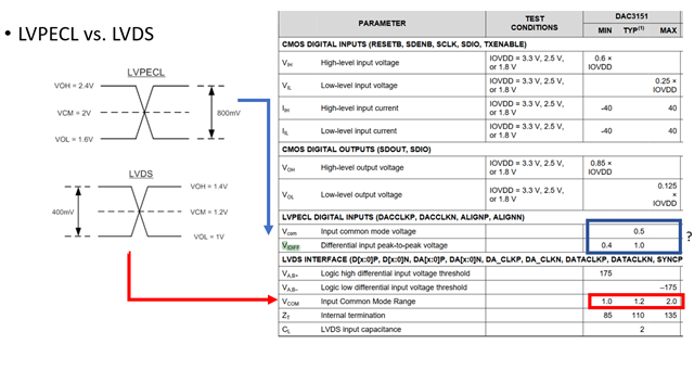

2. I want to use (just as in DAC3152 mentioned) the modulator TRF370417, then I have to match both common-modes (DAC output common-mode is AVDD +/- 0.5V) and from modulator 1.7V. For the DAC3154 we have two different Analog supply voltages (AVDD18 and AVDD33), so which one should we take into considration for the output common-mode voltage (This was already discussed in this question: https://e2e.ti.com/support/data-converters-group/data-converters/f/data-converters-forum/462985/dac3152-output-level-low)
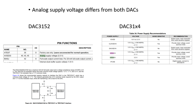
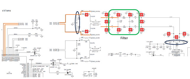
Here's my initial schamtic for the DAC3154, but I need still to figure out both these uncertainties:
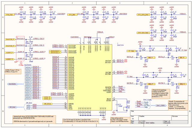
Any help would be much appreciated!

3058.DAC.pdf

  • Hi Danny,

    Please find design files attached including schematic and .BRD file: DAC31X4EVM_B_DesignFiles.zip

    Regarding your questions, the clock input is self biased. You will ac couple the signal with 0.1uF capacitors and DAC will take care of the rest. If the DAC is supplied a lower swing signal, the slew will inherently be lower on that signal and thus create a possibility for higher levels of aperture jitter which may degrade performance slightly. This is why performance improves on most ADC and DAC when clock levels increase.

     The DAC3152 is low power variant of this device and as a result is not a good comparison resource. The compliance range for the DAC3154 is listed as 1V. So at 20mA fullscale, using a 50Ω termination, Vout max = 20mA *  50Ω (100Ω diff, 50 off each leg to GND) will provide 1V on each single leg or a 2V diff. Does your application require DC coupling the DAC output? If not, ac couple the dac output after the termination resistors and then bias the TRF side of the diff pair with bias tee or inductor.

    Regards, Chase

  • Thank you very much for the quick response!

    The schematic was helpful, but the layout print is a bit too small, so I can't read it well. The .brd file seems to be corrputed. I tried to open in it in Eagle and Altium and I'm getting an error of corrputed data.

    The clock issue is generally cleared. I'm still a bit confused about the termination of the DAC output and TRF input. So no common-mode matching is done here? The TRF needs a 1.7V common-mode at the input, or does the DAC already provides this voltage?
    For the DAC3152 is was the analog VCC, that set the output voltage. In the schematic I followed the trace of the output and just like you said the 50Ohm resistors (on each leg to GND) is placed once on DAC Output side and once again at TRF input side next to the chips. I don't see any AC coupling here too.

  • Hi Danny,

    Sorry for such a late response, the BRD file seems fine on my end when opened with Allegro PCB Editor Viewer. I have never been successful with opening brd files in anything other than an allegro viewer. Regarding the termination between the DAC and the TRF, I am checking with our team for any comments there. Stay tuned.

    Thanks, Chase

  • Hi Danny,

    I am reaching out internally to find out the appropriate group that can help answer the question on the TRF.

    I will update you tomorrow.

    Regards,

    Rob

  • Hello Danny

    The TRF needs a 1.7V common-mode at the input, or does the DAC already provides this voltage?
    For the DAC3152 is was the analog VCC, that set the output voltage. In the schematic I followed the trace of the output and just like you said the 50Ohm resistors (on each leg to GND) is placed once on DAC Output side and once again at TRF input side next to the chips. I don't see any AC coupling here too.

    The user will need to adjust the external resistor network to provide the 1.7V VCM to the TRF370417

    The DAC3154 (ending with 4) and DAC3152 (ending with 2) are two different family of DAC.

    For the DAC3154, I do not think we (TI) ever released this version. The main core is DAC3174 (14bit).

    The DAC3174 is a current source based DAC with compliance of +/-0.5V with respect to the GND.


    Therefore, the following section of the app note can be re-used for the interface for the TRF370417

    https://www.ti.com/lit/ug/slua647a/slua647a.pdf

    refer to section 5 for detail.

    The DAC3152 is current sink DAC with compliance of +/-0.5V with respect to AVDD.

    You can refer to the following app note for interface recommendations.

    https://www.ti.com/lit/an/slaa399/slaa399.pdf

    section 4.1

  • Hello, thanks for the answer!

    I deceided to use the current sourcing DAC3154 with compliance range to 1V. In the schematic  sent here, I can see that the voltage first divided at the DAC stage to half with 50Ohm resistors and again at TRF3705 to half with 50Ohm resistors, so the common voltage at the modulator is 0.25V. Would this be correct to my understanding? I would only need these two resistors along with ac-coupling capacitors, if I don't want any filtering in between?

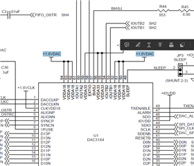
    I spotted another mistake in the schematic/Datasheet. The pin 51 is tied to VDDA18 (+1.8VDAC), but in the datasheet this is an NC (Not used. These pins can be left open or tied to GROUND in actual application use.)

    Same thing for the pins 62 & 63

    Can you explain this?

  • Hi Danny,

    The above would be the correct answer.

    I deceided to use the current sourcing DAC3154 with compliance range to 1V. In the schematic  sent here, I can see that the voltage first divided at the DAC stage to half with 50Ohm resistors and again at TRF3705 to half with 50Ohm resistors, so the common voltage at the modulator is 0.25V. Would this be correct to my understanding? I would only need these two resistors along with ac-coupling capacitors, if I don't want any filtering in between?

    I will refer to to answer your second question

    -Kang

  • Hi Danny, 

    Just to be more clear, it might help to redraw the circuit interface you are proposing.

    Thanks,

    Rob

  • Hi Danny,

    Regarding the pins which are labeled as NC, I suggest to leave these floating. Whenever you come across a discrepancy between schematic symbol and the datasheet, it is always recommended to use the information provided in the datasheet as it will have the most correct and up to date information.

    Thanks, Chase