This thread has been locked.

If you have a related question, please click the "Ask a related question" button in the top right corner. The newly created question will be automatically linked to this question.

ADS1220: ADS1220 set frequency inconsistent with output data rate

Part Number: ADS1220

Dear Expert

Due to the inconsistency between the configuration frequency and output data rate of the ADC chip ADS1220IPW in the pressure detection board, the board cannot be used normally.
Exception description:
The DR bit of software configuration register 1 is configured to be 110 in normal mode, with a theoretical data rate of 1000sps according to the specifications, using continuous conversion mode. Batch chip output abnormality occurred, range: 970-1301sps; Abnormal materials account for 10%.
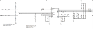
The schematic diagram of ADS1220 is:


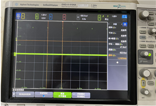
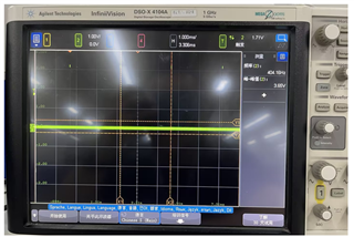
Abnormal board, DRDY outputs frequency waveforms in 1000sps and 330sps configurations respectively:


Troubleshooting points:
1) Remove the resistance of CLK pulled down to ground, 0R, and maintain the abnormal frequency;
2) Remove the series resistance, pull-up resistance, and filtering capacitor related to DRDY, keeping the abnormal frequency unchanged;
3) Heating up ADS1220 results in a change in DRDY frequency and an increase in frequency.

  • Hi Gabriel,

    The schematic doesn't appear to directly correspond with the PCB image.  The probe image shows the scope probe at R26 which in the schematic is the CLK pull-down resistor.  Also it appears that something like a heating iron is be placed on the top of the package to heat the device.  How is this being controlled to make sure that the device is not exceeding the maximum temperature specification?

    The DR bit of software configuration register 1 is configured to be 110 in normal mode, with a theoretical data rate of 1000sps according to the specifications, using continuous conversion mode. Batch chip output abnormality occurred, range: 970-1301sps

    The listed data output rates are not exact and are often rounded off to a near value.  The actual conversion times are listed in Table 11 of the datasheet.  In normal mode and continuous conversions for 1000sps, the actual conversion time is 4144 tclk periods (tclk = 1/fclk = 1/4.096Mhz).  The actual nominal output rate is 988.4sps and is typically +/-1% but can be as much as +/-2%.  970sps would be within the operating range, but 1300sps is a bit high.  I would recommend that the oscilloscope shots be take in single-trigger mode and not auto-triggered mode and then be measured.  This will eliminate any scope retracing issues.  I would also recommend that the best possible scope resolution be used to get the best accuracy in the measurement.  Also, the measurement should be take from one falling edge of DRDY to the next falling edge of DRDY.

    The CLK pin is a digital input pin, so the main point here when using the internal oscillator is to prevent the CLK pin from floating.  When not providing an external clock,  you can directly connect the pin to ground if you wish.

    One other consideration is making sure you follow the DVDD ramp timing shown in section 10.2 of the datasheet.  If the timing  is not met the device may not be in the correct operating state, and a RESET command should be issued to restart the device.  I would recommend using the RESET command to see if oscillator timing changes.

    Best regards,

    Bob B