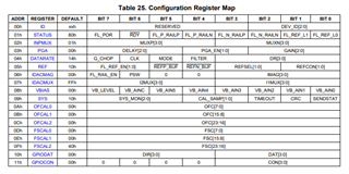
This thread has been locked.

If you have a related question, please click the "Ask a related question" button in the top right corner. The newly created question will be automatically linked to this question.

ADS124S08: Read ADC From ADS124S08

Part Number: ADS124S08

Hi,

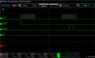
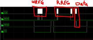
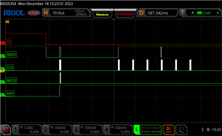
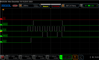
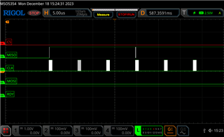
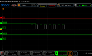
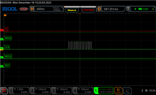
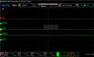
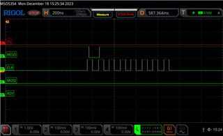
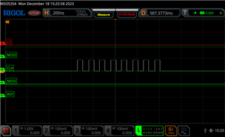
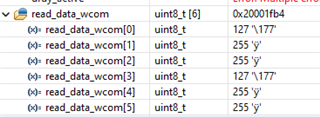
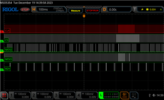
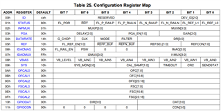
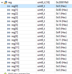
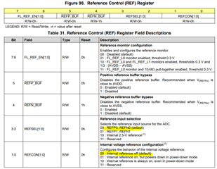
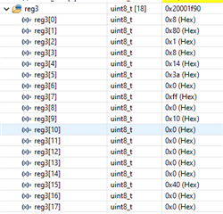
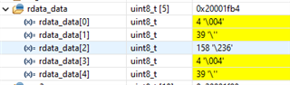
I'm using STM32 microcontroller. I don't understand the ADC reading from ADS124S08. I can communicate the device with SPI and send register map command and then I can receive the all data which is the register map.

I use the AIN0 and AIN1, how can read this data?

  • Hi TI,

    I set also gain to 16 but I can not RDATA also. What should I do?

    Here is my steps;

    - Read the default gain.

    - Write register for gain 16.

    - Read gain which I set.

    - Read data via RDATA command.

    Is there any problem about the steps?

    Edit:

    DRDY is not going to low state.

  • Hi Emre ARSANACI,

    In the sequence you describe (read, write, read), do you get the correct result? Are you able to successfully write to the ADC and then read back the register showing that the write occurred correctly?

    Can you provide logic analyzer plots showing the behavior of the digital communication lines (CS, DRDY, DOUT, DIN, SCLK, etc.)? This will help us understand what information you are sending to and receiving from the ADC.

    -Bryan

  • Hi Bryan,

    Yes you are right. I read the default gain which is 0x00 and write again to gain 16 which is 0x0C and I read this value.

    Here is the plots;

    Write - Read process; (All communication)

    Write Gain; 

    1st byte : 0x43 (because of the write reg = 010r rrrr  Gain is 03h so 0100 0011)

    2nd byte: 0x00 (number of register - 1 = 0)

    3rd byte: 0x0C (because of the 000= tmod default 01: PGA enable 100: Gain 16 equals to 00001100 = 0x0C)

    Read Gain with 0x23 command; (Query)

    Read Gain (Response);

    Notes: When I try to read 1 byte reading gain, I got 0x00. Then I read 2 byte response is correct 0xC.

  • Hi Emre ARSANACI,

    I am a bit confused what you are showing me. I interpret your communication as shown in the image below:

    • The first 3 bytes are the WREG command
    • The second 2 bytes are the RREG command (note the command definition for a RREG is 2 bytes)
    • The last byte is the RREG data, which is correctly showing that the gain is 16

    What is the issue you are having then?

    Have you tried applying a signal and seeing if the output is gained up by 16?

    -Bryan

  • Hi Bryan,

    You are right. I wrote it wrong. 

    I connected the thermopile to AIN0 and my problem is when I try to read data with RDATA command, I got zero from all bytes.

    What is the actual step to read ADC value? 

    Correct me if I am wrong;

    I use the continuous conversion mode and here is my step;

    - Reset the device

    - Write offset to 0x00

    - Wrte gain to 16

    - I read the gain and offset values to verify. ( I got correct value)

    - Send the START command.

    - Send the RDATA command and receive 6 bytes.

    I think I'm missing a step but I couldnt find.

  • Hi Emre ARSANACI,

    Can you provide a scope capture of your data transaction similar to how you did for the WREG and RREG? This was very helpful

    Please show the overall transaction as well as a close up of each individual transaction

    Also, how are you determining when to read data? You should wait for the DRDY pin to transition from high to low, this is what indicates that data are ready to be read from the ADC. It sounds like you might be reading too early, which is why you are getting all zeroes

    -Bryan

  • Hi Bryan,

    Here are the scope captures;

    RDATA Command and Receive Part

    Sending RDATA Command

    Receive Data Part

    Receive 1st byte

    2nd Byte

    3rd Byte

    4th byte

    5th byte

    6th byte

    Let me explain what I did and what I get. 

    I tied 1V to AIN0 and set the gain 1, offset 0 for catching some value. 

    Tied the CS pin to low and send RDATA command (0x12) and wait the DRDY pin to low. When DRDY is low, receive the 6 bytes data and I got 127- 255- 255 -127 -255 -255.

    I repeat the process I mentioned above. In the while block I send the RDATA command and wait again the DRDY to low and take the receive data.

    Please explain how should I use the RDATA command? 

    If the datas are correct how can transform the data or how can I analyze the data?

    Thank you for your response.

    -Emre 

  • Hi Emre ARSANACI,

    What is your SCLK speed? From the scope plots is look like it is ~10MHz - can you confirm? If so, can you try slowing this down to something like 8 MHz and see if the situation improves. Communicating at 10 MHz is right at the maximum SCLK frequency, so any variation in this frequency could cause timing issues

    The general procedure you are following appears to be correct, as are the commands. I cannot see when DRDY transitions low, but it starts low and then transitions back to high as soon as you issue the first SCLK, which is the intended behavior. So this is good

    If you continuously convert, do you see DRDY pulses that are at approximately the data rate?

    What register settings are you using? Since the RREG command is working, can you read back the ADC register map so we can be sure you have the device setup correctly?

    -Bryan

  • Hi Bryan,

    Yes you are right SCLK is 10MHz. I changed with 5MHz and result is same.

    I added the status byte to RDATA command and then I read the status byte with RREG and two of them are same.

    If you continuously convert, do you see DRDY pulses that are at approximately the data rate?

    - I can not understand clearly what do you mean but here is the DRDY pin behaviour. 

    What register settings are you using?

    Input Multiplexer Register : Default

    Gain Setting Register : (000 01 000) Default conversion delay, PGA enabled, Gain  = 1

    Data Rate Register : Default

    Reference Control Register: Default

    Excitation Current Register 1: Default

    Excitation Current Register 2: Default

    Sensor Biasing Register: Default

    System Control Register: Default

    Offset Calibration Register 1: 00

    Other registers set default.

    ADC Register Map

    - I don't know what is the ADC Register Map? Which command or register address to use with RREG?

  • Hi Emre ARSANACI,

    What reference voltage are you using? And how have you applied the reference voltage to the ADC? Can you please provide a schematic of your system

    What does "Offset Calibration Register 1: 00" mean? I would not have expected you to change the value in this register. Can you please let me know what value (in hex) you are writing to the OFCALx registers?

    ADC Register Map

    - I don't know what is the ADC Register Map? Which command or register address to use with RREG?

    I was just asking you to read back all of the registers from the ADC so we can see what you programmed them to be. You can do this by sending a RREG command, and then for the number of registers choose 18. So that would be RREG = 20 12 (RREG command, starting from register 0, reading 18 registers)

    -Bryan

  • Hi Bryan,

    Here is the RREG command result.

  • Hi Emre ARSANACI,

    Thanks for including this info. I can see that you have the REF register (0x05) set as the default, which means the reference voltage source is REFP0/REFN0, and the internal VREF is off. However, your schematic is showing that nothing is connected to REFP0/REFN0, which is why your data is all 1's. You are getting a positive full-scale voltage because VREF = 0, so even the ADC's offset voltage will appear as a full-scale.

    You either need to add a voltage to REFP0/REFN0 or turn the ADC internal VREF on

    ...

    -Bryan

  • Hi Emre ARSANACI,

    Thanks for including this info. I can see that you have the REF register (0x05) set as the default, which means the reference voltage source is REFP0/REFN0, and the internal VREF is off. However, your schematic is showing that nothing is connected to REFP0/REFN0, which is why your data is all 1's. You are getting a positive full-scale voltage because VREF = 0, so even the ADC's offset voltage will appear as a full-scale.

    You either need to add a voltage to REFP0/REFN0 or turn the ADC internal VREF on

    -Bryan

  • Hi Bryan,

    You are right I set the internal ref. and take the data but I have one and last question.

    Here is my register and settings.

    I tied the 100mv from oscilloscope to AIN0 (positive terminal) and AIN1 (negatif terminal from oscilloscope) and get this value.

    How can I make sense of this data? I dont understand the data format actually.

    Thank you for your helping.

  • Hi Emre ARSANACI,

    Since you have both CRC and Status byte disabled, you will only get out 24 bits of data from the ADC. Please see section 9.5.2 in the datasheet for information about how the data maps to the input voltage

    Basically you will get 24 bits of data that your controller will show you as either decimal or hex (looks like decimal in your screenshot). If you separate this out into 3 bytes, then you will need to combine them back together as one 24-bit value. Then you can use the mapping in section 9.5.2 to determine what voltage you measured

    -Bryan

  • Hi Bryan,

    Yes, I've analysed section 9.5.2. 

    According to equation;

    If I set the gain to 2, will my FS value be 1.25v or what?

    Then according to this table

    If I tied the 1.3V to AIN0 and AIN1 will I get the 7FFFFF?

    Can you enlighten me on this?

    Thanks.

    -Emre

  • Hi Emre ARSANACI,

    If I set the gain to 2, will my FS value be 1.25v or what

    Positive full scale (+FS) = 1.25V if VREF = 2.5 and gain = 2. The full-scale range (FSR) extends +/-VREF/gain for this ADC. Therefore, the positive half of the code range (000000h to 7FFFFFh) extends from 0 to +1.25V, and the negative half of the code range (000000h to 800000h) extends from 0 to -1.25V (in this example)

    If I tied the 1.3V to AIN0 and AIN1 will I get the 7FFFFF?

    Are you asking if you tie AIN0 and AIN1 to 1.3V, what will you get? Keep in mind the code range is with respect to your differential signal VIN, where VIN = (AINP - AINN). So if you apply AIN0 = AIN1 = 1.3V, then your differential voltage = 0V. You should therefore expect a code of approximately 000000h, though it will probably be slightly higher or lower due to the ADC offset

    As an FYI, we will be off next week so please be patient with additional queries until the first week of January

    -Bryan

  • Hi Bryan,

    Are you asking if you tie AIN0 and AIN1 to 1.3V, what will you get? Keep in mind the code range is with respect to your differential signal VIN, where VIN = (AINP - AINN). So if you apply AIN0 = AIN1 = 1.3V, then your differential voltage = 0V. You should therefore expect a code of approximately 000000h, though it will probably be slightly higher or lower due to the ADC offset

    Yes, I know. AIN0 and AIN1 difference is 1.3V not a  AIN0 = AIN1 = 1.3V. However when I tied the Vin= 1.9V (Vin = AINP-AINN) I get the 7FFFFF. I cannot get 7FFFFF when there is a value less than 1,9V difference.

    Since +FS is +1.25, shouldn't I get 7FFFFF when I connect 1.3V? 

  • Hi Emre ARSANACI,

    Due to the holiday week here in the US, please expect a response during the week of January 2. Thanks for your patience

    -Bryan

  • Hi Emre ARSANACI,

    Since your original question has been resolved, I moved your new question to a new post: https://e2e.ti.com/support/data-converters-group/data-converters/f/data-converters-forum/1308441/ads124s08-issues-with-reading-data-from-ads124s08

    Please use this link for support

    -Bryan