A related question is a question created from another question. When the related question is created, it will be automatically linked to the original question.
If you have a related question, please click the "Ask a related question" button in the top right corner. The newly created question will be automatically linked to this question.
Could you please help provide a step-by-step guideline that can help customer understand how to do calibration using register 0x08, 0x09 and 0x0A of this device?
Measure the DAC Output at code values a bit away from zero-code and full-scale (ex. 0x1000 and 0xE000)
Calculate the slope of the measured points
Compare these values and slope to the ideal/desired values and slope
Calculate your calibrated GAIN and OFFSET
Select your channel by writing to 0x03
Enable Calibration by writing to 0x08
Calibrate GAIN by writing to 0x09
Calibrate OFFSET by writing to 0x0A
As an example, let's say we are in the 0 - 24 mA output range. 1 LSB size is 0.3662 uA. The ideal values at 0x1000 and 0xE000 are 1.5 mA and 22.5 mA.
Let's use measured values of 1.45 mA and 22.3 mA. We need to offset it by 0.05 mA. Dividing this by the LSB gives about 136 LSB, so we can write 0x0088 to the OFFSET Register.
Our new offset measured values are 1.5 mA and 22.35 mA. Dividing the ideal value by our measured value can give us an estimated gain. 22.5 / 22.35 = 1.0067.
Every LSB in the GAIN register is about 0.00001526, centered around x1 at 0x8000. This gives a GAIN register value of 0x81B7.
Let me know if there are any other questions or if I need to clarify more!
1. Is there a sequence for zero and span calibration? Will there be any impact? 2. So if we only calibrate Span (not calibrate Zero) and only calibrate the middle value and Span, is it possible that the chip can achieve the ten-thousandth specification?
1. There isn't really calibration for zero code error, other than using a negaitve VNEG supply and/or using a bipolar output range, if that is what you are asking. 2. Can you elaborate on what you mean by calibrating Span?
2. So if we only calibrate Span (not calibrate Zero) and only calibrate the middle value and Span, is it possible that the chip can achieve the ten-thousandth specification?
is mean achieve the ten-thousandth specification --> 14bit signal range ---> 16384 LSB level can be detect ? They want no matter positive or negative, both have >10000 LSB, is this achievable ?
Add some questions :
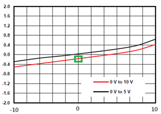
1. For example, when calibrating 0-10V and calibrating 5-10V, will the slope obtained be different when applied to the DAC8775? 2. Can the same slope be applied to Bipolar? Or do the positive and negative values need to be calibrated separately? 3. Assume that in Bipolar, only -10V and 10V are calibrated, or only 5V and 10V are calibrated, and a red line is obtained. If this slope is used to fit the DAC8775, will there be any problem with 0V?
Besides the above questions. Update some issue we are debugging now.
Let me sort out the problems we encountered here. Customer produced 120pcs, and 20pcs failed with the 0.01% correction. When initial power on output 0V without correction. Normal board: output about 0.2~0.4mV Abnormal board: output 75mV
Their FW team has made several modifications 1. The machine needs to be heated for 30 minutes.
2. Originally, FW only calibrated Span, now theyadded a zero correction mechanism, but since the correction of 0V would not be effective, so the zero correction was changed to a correction of 75mV, and then use mathematical operations to find the zero point.
3. Although this method can be calibrated, the entire production time becomes very long and the production cost increases a lot. That’s why customer asked us the question in above.
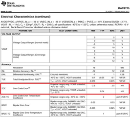
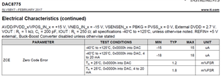
In addition, the normal Zero code Error deviation of TI DAC8775 is plus or minus 2.5mV. Why some of these chip have a deviation of 75mV at initial power on ?
In addition, the part that needs to warm and waite 30 minutes is also strange.
The ppm FSR/°C numbers in the Datasheet are very small. Can you help me confirm whether the DAC8775 needs to be warmed up when calibrating?
Since the calibration steps for Offset are based off of LSB size, you will likely have to update your offset and gain calibration values if you are changing the scale.
Can you share the schematic of the abnormal boards that you are observing?
Since the calibration steps for Offset are based off of LSB size, you will likely have to update your offset and gain calibration values if you are changing the scale.
Can you update these process into the step what you have provide in the history ?
Since different output scales use different/additional circuits inside the device, the amount of LSB needed to calibrate may need to be changed. I would recommend using all of the steps each time you change the scale, for the most accuracy.
I can do a small test on the values I get on my EVM, to see the relationship between different scales' calibration values.
When you mentioned the part needs to be heated for 30 minutes, what is the customer's reasoning for heating? Does it help resolve the 75 mV issue or something else?
I don't see anything immediately with the schematic. I would verify that when the customer is externally resetting the device at startup, PVDD and DVDD have reached operational voltages.
When you mentioned the part needs to be heated for 30 minutes, what is the customer's reasoning for heating? Does it help resolve the 75 mV issue or something else?
The issue board will have 75mV offset at output when the system just power on, after 30min, this offset will close to 0V. That is why customer said he need to pre-heat for 30min.
If you need a chip to do the FA, please let me know, I'm afraid this is a chip quality issue.
Customer produced 120pcs board this time, and 20pcs failed to pass the 0.01% correction.
And they found, when the system just power on. Normal board: output about 0.2~0.4mV Abnormal board: output 75mV at initial, then need about 30min to wait it's output close back to 0.2-0.4mV.
What DAC output ranges are the customer observing this 75 mV issue? Can they verify that their negative supply and reference voltage are stable/correct during this event?
If this was only tested on one unipolar range, can they check using a bipolar range as well?
If the issue persists, I may ask for an output plot of several points as well.