This thread has been locked.

If you have a related question, please click the "Ask a related question" button in the top right corner. The newly created question will be automatically linked to this question.

DAC81416EVM: DAC61416

Part Number: DAC81416EVM

We are currently developing a design where we control the DAC61416 with a 3,3 V µC (Teensy 4.1). The initial design to achieve SPI communication was with using a level shifter TXU0304 shifting the values to 5 V.

For testing we only try to speak to one DAC board at a time (in the final design there are 13 connected). We later realised that the DAC also works with a 3.3 V logic and therefore, got rid of the level shifters. To verify this functioning, we used DAC81416 EVM board instead and were able to update the channels successfully. When we attemt to do the same thing with the PCB that we designed, we notice that the DAC is powering on, but the channels don't output anything. 

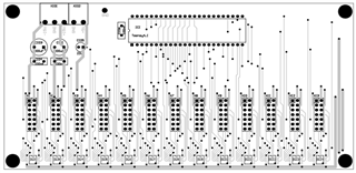
We are having the following design:


Please note: in the schematic, we also have the level shifters which we no longer use. We got a new PCB which directly connects the SPI signals from the controller to the connector and goes to the DAC (which is mounted on another PCB). 

We are using the following code:

****************************************************************************************************************************************************************************************************************************************

#include <Arduino.h>
#include <SPI.h>  // include the new SPI library:

const int CS_pins[13] = {6,7,8,9,10,25,26,27,28,29,30,31,32};
const int CS = 6;


inline void CSON()
{
  digitalWrite(CS, LOW);
}
inline void CSOFF()
{
  digitalWrite(CS, HIGH);
}

void write_reg(uint8_t reg, uint16_t wdata)
{
  uint8_t lsb = ((uint16_t)wdata >> 0) & 0xFF;
  uint8_t msb = ((uint16_t)wdata >> 8) & 0xFF;
 
  SPI.beginTransaction(SPISettings(16000, MSBFIRST, SPI_MODE1));
  CSON();
  delayMicroseconds(10);
  SPI.transfer(reg);
  SPI.transfer(msb);
  SPI.transfer(lsb);
  CSOFF();
  delayMicroseconds(10);
  SPI.endTransaction();
}

void setup()
{
  Serial.begin(9600);
  Serial.println("In Setup...\n");
  pinMode(CS,OUTPUT);
  pinMode(11,OUTPUT);
  pinMode(12,INPUT);
  pinMode(13,OUTPUT);
  //digitalWrite(12,LOW);
  digitalWrite(CS,HIGH);
  //delay(5000);
  SPI.begin();
  // Init SPI0
  Serial.println("SPI0 init...\n");  
  delay(1000);
 
  write_reg(0x03, 0x0084); // SPICONFIG: DEV-PWDWN=0
  write_reg(0x04, 0x3F00); // GENCONFIG: REF-PWDWN=0
  write_reg(0x05, 0x0000); // BRDCONFIG: DACx-BRDCAST-EN=0
  write_reg(0x06, 0x0000); // BRDCONFIG: DACx-SYNC-EN=0
  write_reg(0x09, 0x0000); // DACPWDWN: DACx-PWDWN=0, x={A,B,C,D}
  write_reg(0x0A, 0x0000); // DACx-RANGE=0b0000, i.e. 0-5V
  write_reg(0x0B, 0x0000); // DACx-RANGE=0b0000, i.e. 0-5V
  write_reg(0x0C, 0x0000); // DACx-RANGE=0b0000, i.e. 0-5V
  write_reg(0x0D, 0x0000); // DACx-RANGE=0b0000, i.e. 0-5V
  Serial.println("warte 1 Sek..\n");
  delay(1000);

  Serial.println("Init abgeschlossen");
}

void loop()
{
  //unsigned char bytes[4];

  // Channel 1 is made HIGH for 1 sec and then LOW

  write_reg(0x10, 65535);
  delay(1000);
  write_reg(0x10, 0);
  delay(1000);
  Serial.println("Loop done");
}
****************************************************************************************************************************************************************************************************************************************
Please find the oscilloscope screenshots attached. The first image shows SCLK and CS, the second one shows SCLK and SDI. The third image is the output as seen on the logic analyzer.

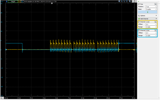
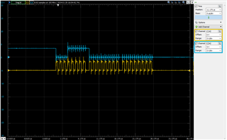
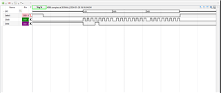
The DAC is switching on and the SPI signals are visible. But the channels are not getting updated and we cannot figure out why.
Would it help in any way if we use DAC 81416 instead of DAC 61416 for our design ? 

Your feedback is highly appreciated. 

Thank you. 
  • Hello, 

    Thank you for your question. Sanjay will review the details and provide a response to you shortly. 

    Best,

    Katlynne Jones

  • Hi Lalita,


    I have looked at the schematic and it's slightly different than the typical schematic provided in the DAC81416EVM' user guide. But I still think, your design should work without any issue. To debug your issue please confirm that- 

    1. you have measured the DAC61416 power supplies and they are within the recommend voltage limits (VCC,VSS,VAA.VDD and VIO) .

    2. you are able to check the SDI lines along SCLK and CS, and that each SPI write is fetching correct data.

    3. you are able to check the SDO line and able to verify if SPI read command is working or not.

    4. you are to enable the internal reference and measure it's value ~ 2.5V.   

    Here is the minimal set of commands to verify the DAC VOUT channels - 

    a) Write 0x0A04 in SPICONFIG (0x03) -  to power-up the DAC81416 device 

    b) Write 0x3F00 in GENCONFIG (0x04) - to use internal reference

    c) Write 0x0000 in DACPWDN (0x09) - to power-up the individual DAC channels

    e) Write 0x8000 in DACn_DATA (n = 0x10 to 0x1F) -  to configure the individual DAC channel outputs to 2.5 V 


    Thanks,

    Sanjay 

  • Thank you for your respose. Here is what I found out:

    1. The power supplies are all within the recommended voltage limis. (Vcc = 15 V, Vss = -15 V, Vaa = Vdd = 5 V, Vio = 3.3 V)

    2. SDI and SDO are working fine (I posted the SDI screenshots in the query above).

    In the DAC evaluation board, we can toggle the reference and see the 2.5-V on J1.7 go on and off. But in my PCB, the VREF pin is not easily accessible to check if the reference is actually turning on or off. Since it is located very close to theREFCOMP and REFGND pins that are tied together to ground in my design, I am unable to isolate and measure the voltage at VREF with a multimeter. If the 0 V that I am measuring, is actually VREF, this might be the problem here. Can I verify if my REF is actually turning on some other way, for instance, by reading out the status of the pin ? 

  • Hi Lalita,

    Are you saying that both the REFCOMP and REFGND pins are connected to pcb GND ? But as per your schematic, REFCOMP pin should have a 330pF cap and that's the correct configuration.  

    Try probing the C104 (REF cap) node voltage, it should be ~2.5V after enabling the internal reference. 

    Regards,

    Sanjay

  • Hi Sanjay, 

    The measured voltage at REF cap is 0 V. We changed our circuit to operate at VIO = 3.3 V, but the LDAC, RESET and CLEAR are still connected to 5V. I am not sure if these pins need to be connected to VIO = 3.3 V too. Do we need to change the voltage at these pins too ? Also, I feel that due to some reason, my DAC is never leaving the POWER-on-RESET state. The registers are always configured to their default values and do not update at all based on the input that I explicitly provide in the code. Please let me know if there is something that is not working out in our circuit.

  • Hi Lalita,


    Please try to change the LDAC, CLEAR and RESET pull-ups to 3.3V (ideally it should matter).

    And also can you please clarify about the REFGND and REFCOMP pin connection, are they shorted to GND ? 

    Still if you are not able to get the device working, let's have a short debug session.


    Thanks,

    Sanjay

  • I will try to change the LDAC CLEAR and RESET pins and see if anything changes.
    And yes, REFGND and REFCOMP pins are both shorted to GND.
    I will get back to you again in case the problem persists even after changing the pull ups to 3.3 V.

    Thank you. 

  • Hi Lalitha,

    REFCMP pin should have a 330pF cap to REFGND. Internal reference will not be proper and device might not respond as excepted If REFCMP pin is connected to GND. Please correct this. DAC81416

    Regards,

    Sanjay