This thread has been locked.

If you have a related question, please click the "Ask a related question" button in the top right corner. The newly created question will be automatically linked to this question.

DAC8760: Regarding output data issue

Part Number: DAC8760

Hi support team.

Currently, my customer is having a problem where some of them are outputting output that exceeds the error range specified by TUE in the data sheet.
Since there are some individuals that fall within the TUE regulations, we suspect that the problem is caused by the device.

The data is as follows.
The conditions are below.
・External Rset
・Measured at room temperature Ta=25℃.
・Setting is 4mA-20mA.

Normal measurement values are also listed for reference to show that they are not dependent on the measurement environment.

<abnormal data>

output current(mA) Sample1 Sample2 Sample3 Sample4 Sample5 Sample6
4 3.9805 3.9856 3.9833 3.9903 3.9843 3.99
5 4.9764 4.982 4.9783 4.9882 4.9801 4.9886
6 5.9712 5.9784 5.9745 5.9847 5.9764 5.9847
7 6.9665 6.9744 6.9705 6.9813 6.9729 6.9809
8 7.962 7.9699 7.9657 7.9798 7.9692 7.9799
9 8.9579 8.9657 8.9607 8.9777 8.9651 8.9787
10 9.9528 9.9623 9.9565 9.9742 9.9618 9.975
11 10.9478 10.9592 10.9527 10.971 10.9582 10.9711
12 11.9436 11.9547 11.948 11.9691 11.9543 11.97
13 12.939 12.9502 12.9432 12.9672 12.9504 12.9686
14 13.9338 13.9464 13.939 13.9636 13.9467 13.9647
15 14.9285 14.943 14.935 14.962 14.9432 14.9605
16 15.9238 15.9387 15.93 15.958 15.9391 15.9592
17 16.9196 16.9342 16.9253 16.9562 16.9352 16.958
18 17.9147 17.9307 17.9214 17.9529 17.9319 17.9542
19 18.9096 18.9273 18.9173 18.9494 18.9282 18.9503
20 19.9045 19.923 19.9123 19.9475 19.924 19.9483

<normal data(measured  4mA and 20mA only)>

Sample No. 4mA 20mA
1 3.9968 19.9869
2 3.9994 19.9941
3 3.9979 19.9916
4 3.9982 19.991
5 3.9971 19.9857


The error range specified by TUE regulations is within ±0.1%FSR.
That is, the maximum value is ±16uA.
As you can see in the data, they all fall outside this range.
Normal measurement values are also listed for reference to show that they are not dependent on the measurement environment.

Do you still consider these measurements to be abnormal?
Or do you think that this is happening because our understanding is wrong?

Best regards,

Higa

  • Higa-san,


    For the numbers, they do look like they have some error associated with measurements, but there are some unaccounted errors not covered in the TUE specification. First, the TUE calculation assumes using an ideal external reference. The DAC converts the digital code to a voltage output compared to a reference voltage. If there is an error associated with the reference, this becomes a gain error and should be added to the TUE.

    To account for this, they can measure the reference voltage (internal or external) and scale the output voltage just to check the accuracy of the DAC. This account for error contributed by the reference voltage. Are they using an external or the internal reference? Can they measure the reference back at the same time as making the measurements?

    Another possible error comes from the external Rset. The TUE from the external Rset specification assumes an ideal Rset value. If the Rset tolerance is 0.1%, then this adds to the TUE. If they have an extremely accurate resistor for an external Rset, I would use it. However, I think the internal Rset is better than 0.1% tolerance because it is trimmed.

    I would note that the measurements show some values that are near 0.5% error, which seems a little high. There may be some multimeter inaccuracy, but if you are using a good 6-1/2 digit multimeter, you're measurement error is probably near 0.1%. I would measure the Rset value and measure the reference back and check the error again.


    Joseph Wu

  • Hi Joseph-san

    Thank you for your prompt reply.

    The below are some additional information.

    -Using an internal reference

    -Rset is 15kohm@0.1%

    Best regards,

    Higa

  • Daisuke-san,

    Using the external reference still has an added 0.1% error (coming from 5V ± 5mV in the electrical specifications). Again, even with the external reference, you can still measure it to see how much error it is contributing. For the external Rset, you can't measure the resistance while it's placed in the circuit, but you can use the internal Rset as an option and it may have a similar accuracy because it is factory trimmed.

    Joseph Wu

  • Also, how are they measuring the current? Are they using a multimeter with an ammeter setting? Or are they sending the current through a known resistor and measuring the voltage? 

    If they use the second method, the test resistor also adds some error.

    Joseph Wu

  • Hi Joseph-san

    I confirmed to my customer. 

    -Measuring method : Digital Multimeter(7461A:ADCMT) 

    -Measured REF voltage

    Abnormal(bad) sample : 4.998-5.000V <- good

     -Measured Output accuracy with internal Rset

    There was no change in the data.
    (Maximum error is -0.48%FSR)

    The results show that both offset and gain errors are likely to be worse than the worst in the data sheet.
    Is there anything we need to check additionally?

    Best regards,

    Higa

  • Daisuke-san,

    I'm still not sure why the current measurements are off. Do you know if the voltage outputs are similarly lower? Are you able to send a schematic?

    Joseph Wu

  • Hi Joseph-san

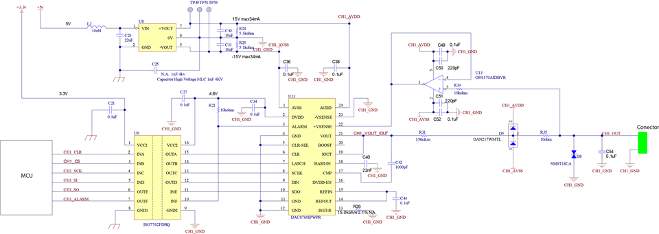
    I attach the Schematic as below.

    The voltage outputs are no problem.(within spec)

    BBest regards,

    HHiga

  • Hi Daisuke-san,

    We are reviewing this and will get back to you shortly.

    Thanks,
    Lucas

  • Hi Daisuke-san,

    Can you describe the register writes/reads that are taking place so I can follow the same steps on my EVM?

    Also, can you try reading back the Status register to verify the device does not have any error conditions noted?

    Thanks,
    Lucas

  • Hi Lucas-san

    >Can you describe the register writes/reads that are taking place so I can follow the same steps on my EVM?

    I don't quite understand your intention. Since this is happening on a board manufactured by the customer, so they have not confirmed the event with EVM.

    Best regards,

    Higa

  • Hi Lucas-san

    >can you try reading back the Status register to verify the device does not have any error conditions noted?

    I confirmed to my customer.

    Status registers are all "0".(no error)

    Regards,

    Higa

  • Hi Lucas-san

    The below is additional information.

    The customer calibrated the offset and gain errors.

    The results are shown below.

    Calibration result.xlsx

    The result is a value larger than the maximum value of INL even after calibration.

    My customer believes that the INL was above specification initially (at the time of shipment).

    This is a question from them.
    - Is the calibration method correct?
    - If correct, are these measured samples abnormal?

    Best regards,

    Higa

  • Hi Daisuke-san,

    Thanks for sharing the results. Joe and Lucas are reviewing and will get back with a response soon.

    Best,

    Katlynne Jones

  • Hi Daisuke-san,

    Based on my reading of the spreadsheet, they are using the endpoints (0 and 16 mA) for their calibration. We don't recommend using endpoints as they are affected by zero-code and full-scale error sources. Choosing codes that are spaced from the endpoints (ex. 0x0400 and 0xFBFF) are recommended. Also, the calibration is also a purely digital one, meaning you would not be able to go past the min and max values you are currently seeing for 0x0000 and 0xFFFF. 

    Here is a snippet from the datasheet:
      

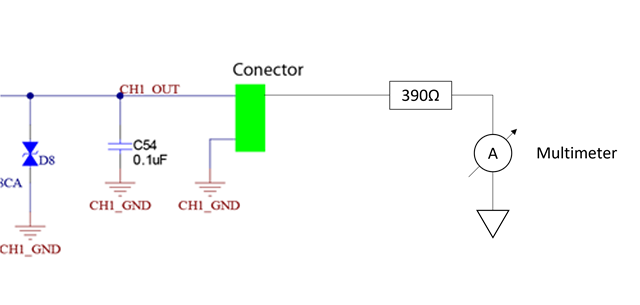
    Is the customer measuring at the green connector or at another point?

    Are they including additional load resistance other than the 150 Ω and 10 Ω?

    I also noticed that the CMP capacitor C42 is greater than 470 pF and should have an additional 100 pF CAP from CMP to GND.
    I don't think this would be the cause of the inaccuracy you are seeing though.

    Thanks,
    Lucas

  • Hi Lucas-san

    I show the measurement point and load resistance as below.

    Digital multimeter : 7461A(ADCMT)

    Best regards,

    Higa

  • Hi Daisuke-san,

    That should be a suitable load, with there being enough headroom for 20 mA to be sourced over 550 Ω.

    Have the AVDD and AVSS the DUT is receiving from U8 been verified to be stable at ±15 V?

    Have there been any ALARM PIN indication with the devices that are having the inaccuracies?

    I also see that the schematic is labeled with CH1, is this specific CH1 where all of the samples are tested or are they in different channels?

    Thanks,
    Lucas

  • Daisuke-san,


    I did take a quick set of measurements on the DAC8760EVM and the device appeared to be in specification. However, I do have some thoughts on what might be cause some error on the DAC.

    First, for my measurements I set the device to the 4-20mA range and set the codes from 0x0000, 0x1000, 0x2000, all the way through to 0xFFFF. Then I measure the current in two different ways. In the first method, I use a 500Ω resistor with a 0.002% tolerance. This gives me an output voltage from about 2V to 10V. This has two benefits. The voltage measurement range can be kept within one range of the multimeter (0V-10V) and I also am able to measure the reference with the same voltage measurement range. If I had a measured in a different voltage range, or used a current measurement, then the gain error might be different compared to the reference measurement.

    The second measurement is a direct ammeter measurement. Because the output range is 4-20mA, I need to use the 0-100mA range of the ammeter, which might have a slightly different gain error. Depending on the meter, this might have a higher error. I use an Agilent 34411A, which is generally very good. Regardless, here are the results in a table.

    Code 500 Ohm 0.002% (V) 100mA range (mA)
    0000 2.0007 4.002
    1000 2.5012 5.003
    2000 3.0006 6.002
    3000 3.5007 7.003
    4000 4.0005 8.002
    5000 4.5008 9.003
    6000 5.0004 10.003
    7000 5.5002 11.003
    8000 6.0002 12.003
    9000 6.5004 13.004
    A000 7.0001 14.003
    B000 7.4998 15.003
    C000 8.0000 16.004
    D000 8.5001 17.004
    E000 8.9999 18.004
    F000 9.4995 19.004
    FFFF 9.9996 20.004

    I didn't plot these values, but you can see that the linearity and gain error are rather good. The reference value itself is 4.9975V, which gives this device a positive gain error.

    When it comes to the customer's gain error, there are a couple of possibilities. The reference and other voltage measurements appear to be correct. Because of this, I'd try to make more measurements with one of the voltage ranges instead of using the direct current measurement. There may be more error because they are measuring with a limited part of the ammeter range.

    Another possibility is that there might be a problem with the current range as well. If they are using an external Rset, then any resistor error becomes reflected in the current output. So if the 15kOhm resistor has a 0.1% tolerance, this could add 0.1% gain error to the output. If there is extra series resistance associated with the Rset (soldering, trace resistance) or extra ground loop voltage, this also adds to the error on the output.

    If the Rset is internal, then I think there is a less likely problem with the current error. For the internal Rset resistor, the value is trimmed at final test and it is trimmed better than 0.1%. The only thing that I think might be an issue is that there is some package stress causing a shift in the resistance value. This might be improved by reflowing the solder on the device (is this a QFN leadless or TSSOP package?). This device does have a thermal pad which I think does help with stress, but I'm not sure. I would also check the reference value. If the reference is at an expected value, then the package stress might not be the problem. The reference is also often affected by package stress.

    If they continue to see this type of error, I would check with them to see if they are able to reflow the solder on the device to see if the gain error changes. There are specified solder temperature reflow profiles to reduce the effect of package stress.


    Joseph Wu

  • Hi Joseph-san

    Thank you for your reply.

    However, we also checked the DMMn range issue and Rset, but as before, there is a large deviation from date sheet spec.
    We are planning to request FA analysis as the device's performance has already deteriorated.

    Regards,

    Higa

  • Daisuke-san,

    Ok, if you do request the FA analysis, I'll close this post. Out of curiosity, did they try to reflow the solder connecting the device to the board?

    Joseph Wu

  • Joshua-san

    yes. They re-implemented it and the problem reappeared.
    On the other hand, they mounted it on a board that had no problem, but the problem was reproduced in the same way.
    From this result we concluded that there was a problem with the device.

    Regards,

    Higa

  • Daisuke-san,

    Ok, thank you. Let me know if you are able to make the FA request.

    Joseph Wu