This thread has been locked.

If you have a related question, please click the "Ask a related question" button in the top right corner. The newly created question will be automatically linked to this question.

ADS1115: The ADS1115 is damaged,please help

Part Number: ADS1115

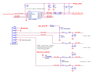
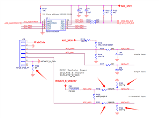
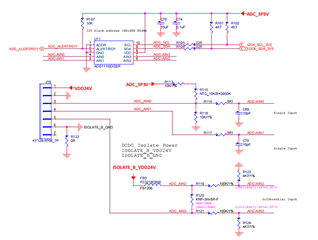
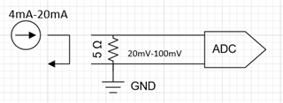
1.Our company's products use ADS1115IDGSR as the ADC function. The product is installed on a liquid transport car, and the J19 connector is connected to the liquid level transmitter.

2.AIN0/AIN1 software is configured as a single -end signal input, AIN2+AIN3 software configuration to differential signal input

3.After the product passes through the aging test, it is installed on the car, and the ADS1115IDGSR function appears abnormal;

4.Products with abnormal function, measure the pins of the ADS1115IDGSR chip, most of them are AIN1/AIN2/AIN3 impedance, and there are short circuits and roads.

5.What is the reason that causes ADS1115IDGSR abnormality? Is there a problem with the hardware design or the software configuration? Annexed ADS1115IDGSR principle diagram, please review and check.

Thanks!

ADC_ADS1115.pdf

  • Hi Jiang,

    If parts are failing after running tests, it is likely that one or multiple recommended operating conditions are being violated, which may result in damage to the part.

    From the data sheet, the absolute max voltage that can be applied to any of the input pins is VDD + 0.3V (which in this case is 3.3V + 0.3V) with respect to GND. Even short transients that exceed the absolute max ratings for a short period of time could damage the part. 

    AIN0 input seems to be within the recommended operating conditions, but I'm unsure about the other inputs. 

    Is 24V being applied to one of the input pins? This would violate the recommended operating conditions stated in the data sheet.

    Best Regards,

    Angel

  • Dear Angel:

    Thanks

    Thank you for your reply so quickly
    I have the following questions:
    1. The voltage entered in Ain1 is 0 to 3.3V;
    2. The input of AIN2/AIN3 is the current signal of the instrument instrument 4MA-20MA, AIN2/AIN3 parallel resistor R120, and the resistance value of 5Ω is 5Ω.
    3. In order to meet the AIN2/AIN3 voltage of 0 to 3.3V, the updated schematic diagram is as follows:

    4. Eliminate the ISOLATE_B_GND through the OR resistance to GND, and divide the pressure through R119/100K and R123/11K, R121/100K and R124/11K; help to confirm whether the updated schematic is OK?
    5. If the current signal of the instrument is 4MA-20MA, use ADS1115idGSR as an ADC chip; is there a better hardware design scheme recommendation? For example, the current collection increases the OP amplifier, and the OP amplifier output is connected to the input of ADS1115.
    Thanks!

    ADC_ADS1115-V1.1-20240403.pdf

  • Hi Jiang,

    This resistor divider network would lower the voltage at the input pins from 24V, which is certain to damage the device, to around 2.38V which is an acceptable input voltage for this device. Make sure that a FSR that allows for this range (such as +/-4.096) is used, as the default FSR is set to +/-2.048V.

    Have any tests been conducted with this modified schematic to verify?

    I would suggest taking a look at some of our reference designs: TIDA-00824 reference design | TI.com for example circuitry for this device, or our available EVM: ADS1115EVM-PDK Evaluation board | TI.com for a schematic and layout example. 

    Section 12 of the data sheet talks about layout guidelines for this device and shows some examples. 

    Best Regards,

    Angel

  • Dear Angel:

    Thanks a lot for the answers

    Please help to confirm again whether the updated schematic is correct and whether the software configuration is correct.

    The current flowing through the ADC_AIN2/AIN3 sampling resistor 5Ω ranges from 4mA to 20mA, that is, the differential input voltage ranges from 20mV to 100mV. Adjust the resistance value of R123/R124 resistance to 4K7, software configuration FSR=±0.512V, and Data rate set to 100:128 SPS (default).

    ADC_ADS1115-V1.2-20240408.pdf

    Thanks!

  • Hi Jiang,

    Angel is currently out of the office for a couple of days.  You can expect him to respond in a few days.

    Best regards,

    Bob B

  • Hi Bob,

    Is Angel back in the office? We look forward to his reply.

    Thanks,

    Leven

  • Hi Jiang,

    I took a look at the new schematic.

    The FSR of ±0.512V should be okay for the range you want to measure (20-100mV). FSR = ±0.256 V would work as well. 

    I see potential problems with having the resistor divider network at the inputs. Having such a large resistance at the analog inputs will cause large errors due to the voltage drop across the input resistor generated by the input bias current of the device. 

    What you could potentially do to measure 4-20mA current across a resistor is to have AINN (ADC-AIN3) of your differential signal be connected to GND as shown: 

    This would keep the absolute voltage at the analog input pins lower than the maximum voltage of 3.3V allowed (ADC-AIN2 between 20-100mV, ADC-AIN3 at 0V) to ensure the device is not damaged.

    Explaining the connections of J19 would also help, as it is not clear if ADC_AIN3 is being connected to ISOLATE_B_GND externally (pins 5 and 6) or what is being done. 

    Best Regards,

    Angel