


Part Number: ADC3541
Other Parts Discussed in Thread: ADC3543
Tool/software:
Hello,
I am creating this new thread, as my previous one (see referenced original question above) has been closed (possibly automatically, due to inactivity) by TI without providing a definite answer.
In the meantime, I am very sure that the datasheet in its current version (December 2022) has multiple flaws.
First of all, to re-cap: we are still trying to get complex decimated data in parallel CMOS mode out of an ADC3543.
Compared to what I wrote in the previous thread, I have made some progress and I can actually read (what strongly looks like) complex decimated data from the chip with BOTH SDR (this is somehow in conflict to the datasheet, which states that "the ADC354x device supports complex decimation output with DDR CMOS interface", but it does not say that it is impossible with SDR CMOS interface) as well as DDR interfaces.
However, the output has almost nothing to do with Figure 8-36 ("Output Data Format in Complex Decimation (default bit mapper)") in the datasheet.
The output looks much more like in Figure 8-37 ("Output Data Format in Real Decimation (default bit mapper)"), but instead of samples A0 and A1 (as written in that figure), I can read alternating in-phase (I) and quadrature (Q) values for the same sample. Replace A0 by I0 and A1 by Q0 to understand how I am currently reading the data.
Also, I am currently only using 14 bits, so not all the pins in Figure 8-37 are in use.
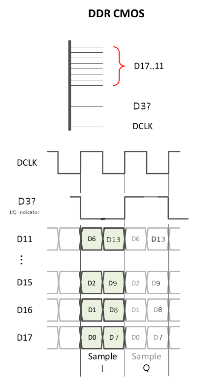
This also finally explains column DCLK of Table 8-4 ("Parallel CMOS Data Rate Examples with Complex Decimation"), which shows double the DCLK rate as expected by looking at (the possibly wrong) Figure 8-36.
Consider the example for N=4 and keep in mind Figure 8-36. Why would the rate of DCLK in a DDR scenario be 32.5 MHz even though the input sampling rate of 65 MHz is decimated by factor 4?
Let us assume the above is correct. Then a big problem arises: How can we know which is the I and which is the Q part of a sample?
With the DDR interface, I have probed several "unused" pins and I have found suspicious DCLK/2 signals on a couple of those pins. Could this be an indicator for whether I or Q is currently output?
There has to be SOME way to find this out, right?
One of these pins is D3/DCLKIN (pin number 35). I added this pin to my design as an I/Q indicator and until know it reliably toggles at the expected DCLK/2 rate.
However, I did not yet test whether this really reliably indicates I and Q, especially after different kinds of resets. So here I need your input: How is I and Q indicated in complex decimation mode? (Please do not answer "By looking at rising or falling edge of DCLK" unless you can also provide initialization examples to achieve exactly what can be seen in Figure 8-36)
So here is a recap of the possible flaws in the datasheet:
- Figure 8-36 ("Output Data Format in Complex Decimation (default bit mapper)") does not seem to reflect the way complex decimated data is output.
If it is possible to achieve the exact output of that figure, please provide some initialization examples that lead to this output.
- DCLK rates of Table 8-4 contradict Figure 8-36.
- Assuming complex decimated output it actually output like I have just described, how can we definitely know if currently I (in phase) or Q (quadrature) data is output on the data bus. Concluding from the above, this is NOT possible by looking at falling or rising edges of DCLK.
Could you please comment on this? It looks like it is possible to get actual complex decimated data out of the chip (in parallel CMOS mode), but NOT in the way as specified in the datasheet.
Best regards.

