ADS1293: GAIN issue and design question - Analog and Digital Filtration - 2 LEAD Holter to pass IEC 60601-2-47

Part Number: ADS1293

Tool/software:

Hej!

I'm having GAIN accuracy issues on a ADS1293 device where I see a offset of about 15-17% from a input signal on the ADS output. 

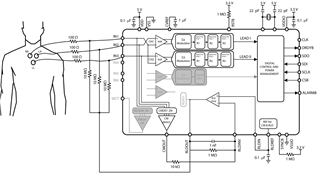
We have a battery powered Holter device for logging ECG data through a 2 LEAD, 3 electrodes configuration, (IN1 = RA, IN2 = LA, IN3 = LL).

We use two channels configuered as:

INA_CH1 = LA-RA

INA_CH2 = LL-RA.

The CMDET is enabled and takes the three IN and routes them through CMOUT to RLDINV through a 10kOhm resistor and to RLDOUT through a 1MOhm resistor. The RLDOUT is routed on the PCB to the three leads with three separete 10MOhm resistors and 150pF caps. 

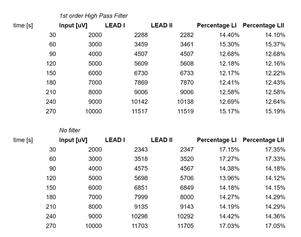
We have a 1st order high-pass butterworth filter in sw which I can enable/disable and edit if possible. The PCB design is pretty much set, we could change some values if necessary. We need to pass IEC 60601-2-47 where the pass criteria for GAIN accuracy is 10%. 

To the question: When I send in a known input signal to the ADS from our signal generator, I get about 15-17% offset on the measuered output compared to the input, both with the digital filter enabled and disabled. The input is a 100ms impulse with amplitude of 2mV-10mV. What could cause this constant gain change? 

  • Hello Pontus,

    Thank you for your post. Would you mind sharing the complete register settings and the ADS1293 portion of the schematic showing the relevant input and RLD circuits?

    Regards,

    Ryan

  • Hello Ryan, 

    Thank you for your quick reply. 

    Here is the relevant part of our schematic with some notes:

    1. On the input, down to the left are TVS diodes for ESD protection.

    2. On the input, there are series resistors of 100 Ohm and on the new design (not measured above) are additional 100k resistors in series on each lead.

    3. You can see the RLD and the connection to the Inputs here.

    I have provided a simplified block diagram below:

    And this is the part of the software which I have currently set to put the output in the middle of the 24 bit measure (tested changing the magic number to 0x800000 as well):

    This is the full register settings:

    ads1293_regdata_t ads_configuration_267hz[] =

    {

    { TI_ADS1293_FLEX_CH1_CN_REG, 0x11 },

    { TI_ADS1293_FLEX_CH2_CN_REG, 0x19 },

    { TI_ADS1293_CMDET_EN_REG, 0x07 },

    { TI_ADS1293_OSC_CN_REG, 0x04 },

    { TI_ADS1293_AFE_RES_REG, 0x00 },

    { TI_ADS1293_R2_RATE_REG, 0x08},

    { TI_ADS1293_R3_RATE1_REG, 0x08},

    { TI_ADS1293_R3_RATE2_REG, 0x08},

    { TI_ADS1293_DRDYB_SRC_REG, 0x08 },

    { TI_ADS1293_CH_CNFG_REG, 0x30 }

    };

    And then for starting conversion I call:

    ads1293_write_reg(TI_ADS1293_CONFIG_REG, 0x01);

    Please let me know if I should try anything differently.

    All the best,

    Pontus

  • Thanks, Pontus. Are all resistor values 1% tolerance? Can you try reducing this to 0.1% and minimize the capacitor tolerance as well? 

    Could you try removing the capacitors and retest?

    Regards,

    Ryan

  • The resistor values are indeed 1%, we are using these: RC0402FR-07100RL for R22, R23 and R24. Is the tolerance important on the RLDOUT (R26, R33 and R38) and CMOUT (R14, R15) as well?

    For the minimized resistor tolerance, is it enough to change C5, C35 and C36?

    Unfortunately, we are a bit limited on tools and space to remove the caps. Are the any other suggestions to try? 

  • What are your thoughts on the register settings and the configuration in general?

  • Hello Pontus,

    The resistor tolerance to the RLD and CM circuits are less critical as those signals become common to the patient. The importance of low tolerance is primarily on the input signal path where common-mode noise can become differential noise due to component mismatch.

    I will come back to review the register settings early next week.

    Regards,

    Ryan

  • Great thank you for your input regarding the tolerances for the resistors and capacitances. 

    I've been running a few additional experiments using the fluke Pro Sim 2 and I am quite surprised to see the same results there. There is a gain difference but I'm not sure if it's the same across a multitude of amplitudes I have not tried that yet.

    For the ads 1293 there is it constant gain of 3.5. I am supplying it with VDD of 3.3 volt. Do I need to scale the converted values from the ads before I can use them?

  • Currently, this is what I do following DRDY:

        // 0. Get data

        uint8_t rx_buff[7];

        ads1293_read_ecg(rx_buff);

        // 1. Normalize data

        int32_t data_i = (int32_t)(((rx_buff[1] << 16) | (rx_buff[2] << 8) | (rx_buff[3])) - 0x798000);

        int32_t data_ii = (int32_t)(((rx_buff[4] << 16) | (rx_buff[5] << 8) | (rx_buff[6])) - 0x798000);

        // 2. Filters

        float lead_it = dsp_HPF_I(data_i);

        float lead_iit = dsp_HPF_II(data_ii);

        // 3. Bring to 16bit range

        int16_t lead_i = (int16_t)(lead_it / 8);

        int16_t lead_ii = (int16_t)(lead_iit / 8);

    No scaling the data with respect to gain, Vref or VDD. Is this correct?

  • Hi Pontus,

    The calculation for ADC output code includes the fixed gain of 3.5 V/V. Therefore, you would have to rearrange the formula below to calculate the differential voltage at the INA inputs:

    As you can see, the output code only scales with the differential input voltage and the supplied reference voltage. VDD is not included in the ADC transfer function.

    Regards,

    Ryan