- Ask a related questionWhat is a related question?A related question is a question created from another question. When the related question is created, it will be automatically linked to the original question.

Tool/software:
But after modifying the gain here, two issues arose. I hope to receive your reply again.
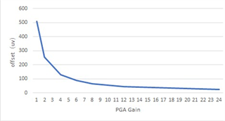
Firstly, I modified the value of the gain and configured it to input short-circuit mode. In this case, the bias voltage does not change much. Configure the CHnSET register to 0x31 (00110001) and 0x61 (01100001). In this way, only changing the gain to 6 and 24, the output voltage value in the input short-circuit mode does not change much, about dropping from 0.5mv to around 0.42mv. It didn't change like the picture you sent me.
Secondly, I configured the CONFIG2 register to 0xD0 and activated the internal square wave signal. When the gain is 1, the values of the square wave signal are+1.36mV and -2.37mV, respectively, instead of the standard+1.875 and -1.875mV. When I change the gain value to 6, that is, configure the CHnSET register to 0x35 (00110101), and change the GAIN value at the actual voltage value where the code data is converted to 6. This formula is double LSB=(2.0 * VREF)/(GAIN * ((1<<24) -1)). At this point, the output square wave signal is 1.788mv and -1.949mv, which is approximately 0.087mv offset from the standard 1.875mv. Change the gain to 24, that is, configure the CHnSET register to 0x65 (01100101), and change the GAIN value at the actual voltage value where the code data is converted to 24. At this point, the output square wave signal is 1.851mv and -1.885mv, which is approximately 0.024mv offset from the standard 1.875mv.
So is this correct? Why configure CHnSET to input short-circuit mode and then modify the gain? The change is not significant and does not match the image you sent me? And when the internal test signal is turned on, the offset of the square wave still roughly matches the situation. May I ask what the reason is? I hope to receive your reply again.
This is the offset voltage of my internal square wave test signal, which was measured by changing different gains.