DAC8742H: Does DAC8742H has passed the physical layer test of Fieldbus foundation

Part Number: DAC8742H
Other Parts Discussed in Thread: TIDA-01504,

Tool/software:

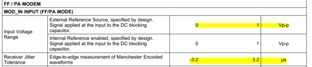
I am developing a fieldbus application using the DAC8742H. The transmitter driver board was taken from the DAC8742H datasheet. However, when I went through the Physical layer tests, it failed at the Receive Jitter tolerance test. I believe the problem is from the DAC8742H itself, because the BUS+ was connected directly to the MOD_IN of the DAC8742H (via DC removal capacitor). I checked the DAC8742H datasheet and found out the jitter tolerance is +-3.2us

However, when setting the jitter of my reference transmitter to 3.2us, the DAC8742H gets only 95-97% of every 1000 transmitted messages. 

So my question is:

  1. Is there any "margin of safety" for the 3.2us jitter tolerance stated in the datasheet? For example, how likely/many percentages, we receive a message correctly if the jitter is 3.21us?
  2. Is the DAC8742H, or any relevant design, like TIDA-01504, passed the Physical layer test?
  • Hello, 

    Joseph will review your questions and provide a response soon. 

    Best,

    Katlynne Jones

  • Hi,


    I'm not sure about the origin of the jitter tolerance specification. For min-max specifications, we generally have some amount of guard band to make sure we're not close to a specification edge case. However, for jitter tolerance, the value may be based on some timing related to an internal clock. I don't think there is a way to guess how likely a message would be received if the jitter is over the specification.

    As for the testing of the device in a Fieldbus application, TI had started work on a design for PAFF but it was stopped due to priority changes in the group. There was a test circuit and TI had worked on a test board and a firmware stack with a third party. As I understand it, the hardware passed all physical layer tests except one test on the input impedance frequency response. There isn't any information on how it did not pass, and any modifications needed make the change.

    There is an older post that does give some information about an example circuit here:

    https://e2e.ti.com/support/data-converters-group/data-converters/f/data-converters-forum/821316/dac8740h-the-reference-design-of-field-transmitter-with-profibus-pa


    Joseph Wu

  • Hi Joseph, great to know that the chip passed all the physical test, including the jitter tolerance test. So it is strange that my jitter test was fail. Could you please share the report on your jitter tolerance test? Did you successful receive 100% of 1000 packages with jitter of +-3.2ms 

  • Thong Tuan,


    I don't have a specific report for the jitter tolerance test. I do have a bunch of log files from a company that started the process of testing the board being developed for Fieldbus.

    To be clear, I'm not very familiar with Fieldbus and how it's tested, so I'm not sure exactly how to help with this question. and I don't know what each of these tests refer to. I'm much more familiar with the HART aspects of this device.

    Regardless, I can check on the origin on the jitter specification and get back to you.


    Joseph Wu

    TI-FF-V301.complete.results

  • Dear Joseph

    Thanks for sharing the test log, but these test are likely relevant to the Datalink layer test, not the Physical test where we check the electrical characteristic of the devices.

    To shorten my question: Texas Instrument stated the chip can tolerance jitter of 3.2us, but my test showed the opposite. So I am asking for document/evidence/test procedure to check if I did something wrong, or the DAC8742H itself can NOT tolerance jitter of 3.2us. 

    Or could I understand that the jitter tolerance has never been tested at TI, but just come from theory/calculation based on the internal clock?

  • Hi,

    I did talk to one of the digital designers, and this specification comes as a percentage of the clock rate (at 31.25kbps, that would be 32us for a bit, and 3.2us would be 10% of the bit period). He thinks that they were able to simulate a 4us jitter error without a problem. However, if the clock source is off, or has additional jitter, that would add to the error.

    Joseph Wu

  • Hi Joseph

    I am now developing devices for PAFF using the DAC8742H. To be able to register the devices for the PAFF protocol compliant/certificate , we need to test or provide the evidence/ documentation to show that the devices could pass the protocol specification. Because TI have stated in the datasheet that the jitter tolerance is 3.2us, could you please send me any proof/statement/ documentation for that, so I can use it when registering for the PAFF certificate? This is very important for me because I have to consider if I should use the  DAC8742H or looking for another solution. 

    Best.

  • Hi Thong,

    We used the Foundation Fieldbus definition of the jitter specification, where we adjusted the midcell edge of every bit in a medium length command.  The jitter variation was implemented at random, but we ensured that some of the edges were >3.2us.  I dont have the distribution, but I recall we did approximately 15% the total bit time, which exceeds the jitter specification.  We send many hundreds of these commands (while changing the jitter every iteration) and then checked for errors across supply conditions and temperature.  We did not see any issues.

    As far as documentation, we would direct you to our specification table in our datasheet as our statement of performance.  As with all devices, we can test and characterize our device to industry norms and under the conditions we specify in our table, as our terms and conditions define.

    So I am interested in why your evaluation failed.  How was your jitter implemented?  Can you share more details?

    Thanks,

    Paul

  • Thong, 

    Also, I was able to find the test report for our board using the DAC8742H. The first test results say that VBUS was 32V, with a waveform of ±3.2us of jitter. The second test results were with VBUS of 9V, with the same jitter.


    For both tests, there were 1000 requests transmitted, and 1000 responses received. Again, this was a board that we put together, but was tested by a third party.

    Joseph Wu

  • Thanks for the report, Joseph. Then I will double check my test to see if I did anything wrong.

  • Hi Paul, thanks for the information. In the test I made, I used a test board to sending a fixed probe node, but the zero crosses in the Manchester code was randomly delayed/preponed 3.2us at some random edges. My device under test, using the DAC8742H, try to capture all the probe nodes. And I received only around 95-97% of each 1000 sending messages 

  • Thong,

    Let us know if you have any other questions. For the time being, I'll keep this thread open so you can post back to it.

    Joseph Wu

  • Hi Paul

    I did the test again but my best result is still 3-5 package lost every 1000. More investigation showed that the DAC chip sent nothing out at the UART when receiving a failed package ( for a good package, the DAC chip start to throw data to the UART just after the first coming data byte). That means the decoding process fail at the preample or the "starting delimiter" can not be detected. In you test, did you add jitter to the whole frame, or just after the starting delimiter?

  • Thong,

    I'm sure that the test adds jitter to the preamble just as it does to the data. The preamble is part of the data frame as well. 

    Is there a way to capture the error from the incoming frame and plot it with an oscilloscope? I think that the transmission and the UART would be offset by the time of a data byte. You can also check the CD pin to see if there is a valid carrier.

    Joseph Wu

  • Hi Joseph

    More investigation indicates that the starting delimiter is very sensitive to the jitter. I used a signal generator to generate 2 testing signal, one without jitter (blue) and the other one has 1 jitter of 3.2us (orange).  Vpp is 0.6V. I configured the DAC to use internal filter, and connect the waveform generator directly to MOD_IN

    In the figure below, you see the 2 waveforms at the bottom part while the top part show the time between all 2 consecutive zero cross (to make sure the timing is correct) .

    The DAC sent 1 data byte to UART with the not jitter signal. 100% stable.

    When sending Signal with jitter, The DAC sent 1 byte to UART also, but not 100%. Example, if I repeatedly send the Signal with jitter 1000 times, interval of 50ms, the DAC will sent data to UART just 600-700 times, meaning around 30% loss. 

  • Thong,


    I'm still not sure what the problem is at this point, but I did have some extra questions.

    How do you generate the jitter in your setup? Do you use a specialized test system? At this point, I don't think I have a test system that could generate this type of jitter. If you have something that does, I might be able to duplicate your issue.

    Also, have you checked the frequency of the oscillator clock? If the oscillator clock is not centered on the correct frequency, the skew of the clock could affect the digital timing and cause a lower jitter to throw up an error.

    It looks like you're just adding an extra 3.2us delay into the middle of the delimiter byte. Just to get a feel for how the device is affected, is it similar when you remove 3.2us from the delimiter? Have you check what happens when you add or subtract different amounts of delay? Have you checked if adding more than one preamble to the start of the frame? I was just checking to see if any of these variations make the better or worse, and to see if the error is symmetric.

    It also looks like you used the DAC8742HEVM to run these tests, is that the case? I just want to make sure that you've tested this with your own board and now with the DAC8742HEVM.

    I'll check with design to see if they have any comments on how they tested jitter and if there are any differences in your tests.


    Joseph Wu

  • Hi Joseph

    I'm still not sure..... -> My problem is that adding 3.2us jitter makes the DAC8742H sometimes can not catch the FF frame

    How do you generate ... -> I used an arbitrary signal generator to generate the FF frame with jitter ( orange line in the above figure). You can reproduce my test with an arbitrary signal generator (I can send the waveform in CSV file)

    Also, have you checked the frequency ... ->  Yes, I measured the output of 4MHz crystal oscillator on the  DAC8742HEVM and it showed exactly 4MHz

    It looks like you're just .... ->  Actually, the jitter test was failed with my self-developed DAC8742H board and my specialized test system. Then I used the DAC8742HEVM board to eliminate all problems (if any) in my self-developed DAC8742H board , still fail. Then I captured the jittered signal (that makes the test fail)  from my specialized test system, re-generated it with signal generator. Finally, with the signal generator, I removed the jitter at several positions ( in the preamble, starting delimiter, main data ), and figured out that even with a single jitter at starting delimiter (showed above), the jitter test still fail. In summary, I tried to simplify the test so that you can re-produce it at TI with a signal generator and a DAC8742HEVM evaluation board

    Have you checked if adding more than one preamble ... -> Not yet, but I can check soon and let you know the result

    It also looks like you used the DAC8742HEVM to run these tests ....-> Exactly, both test with the TI evaluation board and my own board showed the same failure 

    I am very interesting to see if you can reproduce the test at TI and compare the result. You may need a micro controller to count the sending signal from the signal generator ( using the generator's output trigger maybe) and count the UART output of the DAC8742 

  • Thong,

    One thing that I'd like you to change to your test is the method of adding jitter so that an added delay also has the complementary subtraction for each bit. 

    When I first discussed this with the digital designer, he thought that adding a delay within a bit (or a byte) is more of a shift and not jitter. His point was that adding a delay also causes an apparent change in the clock frequency which is somewhat significant even if it is momentary.

    Because you're adding in the shift through basically a lookup from a csv file, you should be able to add a delay within a bit and then remove it at the other side of the transition. This would keep the bit width the same, while adding the jitter in between. 

    Joseph Wu

  • Hi Joseph

    I generated a new jittered signal by moving an edge 3.2us ( orange line in figure below). Still the same 20-30% loss if I send 1000 jittered signals repeatedly (interval 50ms) 

    Another test as you suggested: adding more than one preamble. 100% passed with the blue (no jitter, 1 more preamble added), but still 20-30% loss with the orange (1 jitter of 3.2us, 1 more preamble added),

    Is it possible that you reproduce the test at TI to confirm?

  • Thong,

    I'm looking into whether we can reproduce this test. I personally don't have that much experience with PAFF, and with writing firmware to run this sort of thing, so it may take some time to look at this.

    Joseph Wu

  • Hi Joseph, how 's thing going? Do you able to verify my test? Just let me know if you need anything, such as the testing signal.

    Best 

  • Thong,

    We're still working on this. It's taken a some time to look for our previous testing method and past setup. 

    In the mean time, have you completed the rest of the physical layer tests? Have there been any other issues passing them?

    I'll take any information you have about your testing, and if possible, I'd like to see the schematic as well.


    Joseph Wu

  • Thong,


    I've finally been able to dig up the original testing that we did and I think the discrepancy comes in the method of the insertion of the jitter. We tested the jitter according to the Physical Layer Conformance test from the Fieldbus specifications (FF-830). In this test, they don't add and subtract a 3.2us delay from a single clock edge. Rather, they do successive adds and subtractions of 1.6us to each edge to make the total jitter of 3.2us for any given transition. They show a diagram in the specification to illustrate the nature of the jitter:

    At the end of the specification, they do give a table in Annex C to show a specific timing deviation for receive jitter tolerance. For each 32us increment of communication, there is either a +1.6us or -1.6us jitter added as part of the test for the PAFF Frame:

    I would note that this is an older copy of the specification, so things may have changed. However, I would guess that this is an accurate representation of how the test should be done today. In your case, I think you're adding and subtracting 3.2us of time in the transitions from high to low or low to high. This may be twice the expected value for the jitter itself.

    Regardless, you should consult the test specification and see how the jitter transitions should be implemented.


    Joseph Wu

  • Hi Joseph

    I started with the physical test 2 months ago, using the standard you sent. And the jitter test failed ( the jitter was generated exactly as you showed above). At lot of different jitter signals were created by this method and you will never know which signal makes it fail. So it took me one more month to find out that even with the same specific jittered signal, the DAC chip sometimes can not catch it. Then it took me another month to simplify the problem by indicating that adding jitter at the "start delimiter".

    In short, I tried to simplify the test while waiting for your answer. I was able to pick one of the jitter signal in the Physical Layer Conformance test that causes the failure, and I found out the starting delimiter part in this signal is the problem. If it can not pass my test, it will never pass the Physical Layer Conformance test. But I think you now are investigating from the starting point?

    So, I did the jitter test according to the Physical Layer Conformance test from the Fieldbus specifications (FF-830), and it did not pass. So, what should be the next step?

    I try to simplify the test by using the DAC8742HEVM board with NUCLEO board. I add the code for the NUCLEO board and test set up here  https://www.dropbox.com/scl/fo/0acmv01p0dxfkzgj82l0j/ADUO9nfIZ_tgdkdzThnxQk4?rlkey=3lxade4zxvrsifqtc4h6ncbgh&st=m820yo9g&dl=0 . Also, the good and bad signal was added as CSV file that maybe used to program the signal generator to create the jittered signal.

    With a signal generator, I hope you can reproduce the test quickly. Just let me know if you need more thing

    Best

  • Hi Joseph

    I also added another jittered signal generated as the Physical Layer Conformance test, i.e. add +-1.6us to every zero cross. The DAC chip can not 100% catch this jittered signal. You can find the signal at JitterFullSignal

  • Thong, 

    Normally, we're blocked on our network from dropbox, but I was able to get an exception. I was able to download the two csv files, and the pdf figure, However, I'm still blocked from your zip file, because it's code.

    However, I do have a board working and I did get FF working to write from the device and to read it back correctly. Paul did find the testbench and I think we should be able to test it Tuesday. 

    Joseph Wu

  • Thong,

    I wasn't able to get the 33220A until today, so we're still working on this. 

    Joseph Wu

  • Hi Thong,

    Our goal here is to recreate our validation configuration to dig into this.  As Joe has mentioned, we did pass this jitter requirement and physical layer testing at the time of development and some of our other customers have done so as well.  Your results are surprising to us, but we don't see any flaw in your test methodology to explain it.

  • Hi Joe

    I added a new file TI_Jitter_PASS_123456dotzip.zip . You can unzip this file, rename the extracted file to .zip, and unzip it again with password 123456. Then you can get the code. I hope this can bypass your security block.

    www.dropbox.com/.../TI_Jitter_PASS_123456dotzip.zip

  • Thong,


    The new download was blocked. Security identified it as a zip file and prevented the download.

    I mentioned last time that I found the testbench. This testbench wasn't the exact one used on the DAC8742H, but it was derived from that Labview used to test it. It has controls that set the amplitude, the rise/fall times, frequency, and the addition of the jitter. It also can change the number of preambles, and the data in the transmission. Here's what the controlling Labview looks like:

    I didn't take too many scope shots, but here is at least some of the reception that I got.

    While I am getting some extended results that pass with and without jitter, I still have some problems in getting proper results. The listed frequency from the Labview is a bit off more than I expected, and I do have some cases where I lose communication depending on the preamble and message data. This is both with and without the jitter added to the signal. Right now, I'm just debugging the resulting signal just to make sure that I'm getting the output that is expected, and that the jitter is correctly added in. The jitter is added from an excel file that has the sequence of adds and subtracts from the table in FF-830 that I had copied earlier.


    Joseph Wu

  • The testbench is great Joe. Then you can reproduce my test now. To generate my signal, the jitter table should be like the figure below, where you first prepone the standard signal -1.6us, then add delay +3.2us at the 16th (or maybe the 15th) zero-cross.

    I am very eager to see your result. Please remember to send the same jittered signal 1000 times and count how many pagakes the DAC got.

    Best