This thread has been locked.
If you have a related question, please click the "Ask a related question" button in the top right corner. The newly created question will be automatically linked to this question.
Tool/software:
I am looking for a (probably simultaneous sampling) 8 channel ADC which will be used to rad the output of 8 TIAs (which are used to read photodiode signal levels). I would like >= 115 dB if possible at 1 ksps.
The ADS131E08 seems like a good choice on paper
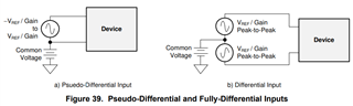
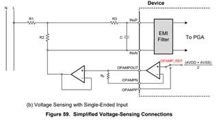
I planned to use the device with a 5V supply (unipolar) the internal 4V reference. I might consider using an external 4.096 V or similar reference if there is any benefit to it. I planned to simply ground the IN#N inputs and use the IN#P pins for the signals. I can't see that it would matter too much that I am only using half the available range, and in any case I couldn't find a better single ended ADC which met my performance needs (I'm open to suggestions). The TIAs would have their gains configured so not exceed 4V at the ADC input. DVDD will be 3.3V
Is there anything about this proposed setup which makes it a bad idea? Will it be able to read signals near 0V correctly?
Hi Adam,
Both ADCs can meet your requirement in terms of 115dB dynamic range, however the negative analog input pin (AIxN) of ADS131E08 should not be connected to the ground under a unipolar power supply because of the input common-mode range requirement. Driving the ADC analog inputs with a pseudo-differential configuration is a good way to measure a single-ended input signal, the dynamic range of the ADCs can be fully utilized too, see the figure 39 from the ADS131A04 datasheet:
ADS131E08 could be a good solution for you as the on-chip OPAMP_REF can be used as the bias voltage as shown in the following figure from the ADS131E08 datasheet (R1 and R2 that form a resistor divider are not needed for your application):
BR,
Dale
Hi Michael,
Thanks much for your feedback.
Using the setup in figure 59 would would add any noise/drift on the power rail to the measurement. I think this would add alot of noise.
My nominal input voltages span 0..4.1V. I could use AVDD=5V, AVSS=0V, the internal 2.4V reference and input a low-noise reference of 2.048 V to all INxN. I think it would work well and use approximately the full dynamic range. Sound right?
One more question about ADS131A04:
ADS131A04 says the inputs can go down to AVSS, even with the charge pump off; is this correct?
Hi,
Using the circuit as shown in the figure 59 can save external DC voltage source and the cost, however you can definitely use an external precision DC voltage for INxN as you mentioned in your proposal.
When the charge pump is disabled on ADS131A04, the absolute voltage on both AinxP and AINxN pin can be as low as AVSS, but you will lose half of the dynamic range.
BR,
Dale
Hi Dale,
To be clear, the voltage setup I requested feedback on above above DOES NOT appear to be valid according to equation 4.
If I put V=2.048 to INxN, and my INxP varies 0..4.096 V then the common mode range is 1.024 ... 3.072
But equation 4 says the allowed CM range is AVDD-0.3-(G*Vdiffmax)/2 ... AVSS+0.3+(G*Vdiffmax)/2 which is approx 1.32 ... 3.68
Hi Adam,
Thanks for your clarification. Your calculation is correct. Holding the INxN pin at a common voltage, preferably at mid supply, is the best solution to configure the fully differential input for a pseudo-differential signal. Since the AVDD of your ADC is an unipolar 5V, I would suggest you to use a precision 2.5V DC for the INxN instead of 2.048V.
BR,
Dale
That still does not work.
There does not appear to be any INxN voltage which will allow the reading of INxP signals outside the range
AVSS+0.3 ... AVDD-0.3
Please confirm.
Hi Adam,
I understood your concern. In order to meet the common-mode requirement in the equation 4, the signal to the INxP should be limited to be less than 0.5V~4.5V, so
Where AVDD=5V, AVSS=0V, Vref=2.4V, 2.5V DC on INxN pin (Psuedo-Differential Input). The measured different voltage Vdiff = ±2.0V.
BR,
Dale