This thread has been locked.
If you have a related question, please click the "Ask a related question" button in the top right corner. The newly created question will be automatically linked to this question.
Tool/software:
Hi Team,
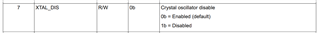
I am facing some difficulties trying to write to the CLOCK register of the ADS131M08 ADC. My goal is to change the XTAL_DIS bit (I am using an external crystal).
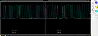
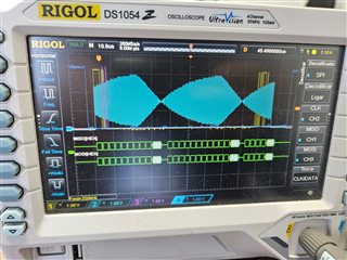
The image below shows the frame that I am sending to the ADC: 0x618000
(WREG), immediately followed by the register data (0x24E
) and 0x00
to meet the word size requirement. However, when reading the register back, its value remains at the default.
Could you please help me resolve this issue?
Hi Lucas,
Can you upload a timing like the following timing including /CS,SCLK,SDI and SDO? It would be good to include the /DRDY signal as well if it is possible. This timing is used to write Gain register (04h address) with 0x0E0E register data.
To be clear, are you planning to set the XTAL_DIS bit in the CLOCK register to '1'? the default value on this bit is '0'. The CLOCK register is defined as Crystal Oscillator Enable, active low. So 0=Oscillator Enabled, 1=Oscillator Disabled.
BR,
Dale
Hi Dale,
Thank you for your reply!
Unfortunately, my oscilloscope has only 2 channels, and I can only measure SDI, SDO, and SCK.
The reason I am setting the XTAL_DIS bit is that I am using an external crystal. The datasheet is a bit confusing because the description for this bit is "Crystal oscillator disable", and by default, it is set to '0' (Enable).
The problem I am facing is that I am not getting any measurements from the channels. I hope this is related to the oscillator, which I believe operates with a clock signal provided by the MCU by default.
Hi Lucas,
If you use an external clock signal provided by the MCU, you are not using an external crystal, so the XTAL_DIS bit in the CLOCK register should be set to '1' to disable the crystal oscillator.
Which channel did you use and you did not get any measurements? When you write 0x24E to the CLOCK register on this ADC, you only enable channel 1 but disable the rest of all channels.
BR,
Dale
Hi Dale,
I tried performing measurements with the default value of the clock register, but I only received the first word (status). All the channels returned null. I issued a total of 9 words (24 bits each) on the SCK line, but I only got the status.
Hi Lucas,
My question was, which channel did you use and you did not get any measurements? When you write 0x24E to the CLOCK register on this ADC, you only enable channel 1 but disable the rest of all channels, so are you measuring and checking the channel 1 or other channels?
BR,
Dale
Hi Dale,
At first, I tried to read the channels that are active by default—according to the reset value of the CLOCK register, all channels should be enabled. After DRDY went low, I pulled the CS pin low and then issued a 9-word (24-bit) command on the SDK line. However, it did not work—all the channels were returning null from the ADC, and I was only receiving the status.
Given this behavior, I analyzed the datasheet and noticed an ambiguous sentence regarding the "Crystal oscillator disable" in the description of the XTAL bit in the CLOCK register. As a result, I began experimenting with changing the XTAL and channel enable bits to see if it would make a difference.
Hi Lucas,
Thanks for your information.
Do you have an external clock (oscillator or clock from CPU) you can use to check? I do not have a Crystal so I can not check it for you. My understanding is, your register reading including other registers was correct, let me know if my understanding is incorrect. What's your SCLK frequency and Crystal frequency? Did you try to program other register and read it back to check? you timing and schematic will be very helpful to identify the issue, you can use different captures for /CS,SCLK,SDI and SDO signals. You can use the configurations to collect the data without writing any registers.
BR,
Dale
Hi Dale,
I have a 7.68 MHz crystal and I am not able to feed the clock with the MCU, just with the crystal. My SCLK frequency is 2.5 Mbits/s.
An update:
I finally managed to write to the registers correctly. It seems the issue was related to my code. After changing the state of the XTAL bit, the DRDY pin stopped oscillating. It appears that the default value of the register is correct when using an external crystal. However, I am still unable to perform channel readings.
In the picture below, I powered up the ADC without changing any register values and issued 3 words (9 bytes) on the SCLK (CH2, light blue trace) just before DRDY (CH4, blue trace) went low. As you can see on the MISO signal (CH1, yellow trace), I only receive the first status word, while the following data are all NULL. These values should be anything but NULL.
Can you help me resolve this issue?
Hi Lucas,
/DRDY is the signal to indicate whether the data conversion completes or not. Low /DRDY means the data is ready and you can read. From your timing, you are sending SCLKs during the /DRDY is high, this is incorrect. The /DRDY signal from the ADC can be used as an interrupt to you microcontroller, the falling edge of /DRDY can trigger the interrupt and then you can send SCLKs to the ADC in the interrupt subroutine.
Also, more SCLKs should be sent to the ADC to read all channel data. 10 words (30 bytes) are expected to shift out the STATUS word+all channel data+CRC.
Your actual data rate is ~3.76ksps based on your crystal frequency and the default OSR=1024. This indicates that you need to read all data during 265us. Your 2.5Mhz SCLK frequency is too low to read the data. You need to increase your SCLK frequency. Maximum SCLK frequency is 25MHz when DVDD is 3.3V.
Are you toggling the /CS when you send the SCLKs to the ADC?
BR,
Dale
Hi Lucas,
In order to read 10 words in one frame, 10*24*(1/2.5M)=96us is needed. 265us is total sample period including high /DRDY time. From your timing, you can see the low /DRDY is short. You can check the actual low time of the /DRDY from your oscilloscope. You will have to send all SCLKs to the ADC when the /DRDY is low.
BR,
Dale
Hi Dale,
Is there any way to increase the low-level duration of DRDY? As shown in the oscilloscope screenshot I previously sent, this duration is less than 5 µs for an OSR of 1024. I have an MCU running at 80 MHz, handling the signal via an interrupt, but it’s still not possible to issue the SCLK before DRDY goes high again
Hi Dale,
I am following the sequence below. Could you help me identify where the mistake is?
uint8_t reset[30] = {0};
reset[0] = 0x00;
reset[1] = 0x06;
reset[2] = 0x00;
HAL_Delay(10); // 10ms delay
HAL_GPIO_WritePin(SPI3_CS_GPIO_Port, SPI3_CS_Pin, RESET);
HAL_SPI_Transmit(&hspi3, reset, 30, 100);
HAL_GPIO_WritePin(SPI3_CS_GPIO_Port, SPI3_CS_Pin, SET);
uint8_t dummy[30] = {0};
drdy_flag = 0;
while (1)
{
if(drdy_flag == 1)
{
HAL_GPIO_WritePin(SPI3_CS_GPIO_Port, SPI3_CS_Pin, RESET);
HAL_SPI_Receive(&hspi3, dummy, 30, 10);
HAL_GPIO_WritePin(SPI3_CS_GPIO_Port, SPI3_CS_Pin, SET);
for(uint8_t i = 0; i<sizeof(conversion); i++)
{
conversion[i] = dummy[i];
dummy[i] = 0;
}
for(uint8_t i = 0; i<9; i++)
{
channel[i] = (conversion[3*i] << 16) | (conversion[3*i+1] << 8) | conversion[3*i+2];
}
drdy_flag = 0;
}
}
The response I get from the ADC is always the following:
1st word: 0xFF2800
2st word: NULL
3st word: NULL
4st word: NULL
5st word: NULL
6st word: NULL
7st word: NULL
8st word: NULL
9st word: NULL
10st word: 0x95E400
The SPI is running at 2.5 MBits/s (I also tried 20 MBits/s, but the response was the same). I am still unable to measure the CS pin and am working around that. All registers are at their respective reset values.
Hi Lucas,
Is there any way to increase the low-level duration of DRDY? As shown in the oscilloscope screenshot I previously sent, this duration is less than 5 µs for an OSR of 1024. I have an MCU running at 80 MHz, handling the signal via an interrupt,
DL: Your data rate is 3.75ksps that is around 266us period for the /DRDY of the ADS131M08. I'm not sure why your /DRDY low time is so short and it is less than 5us. Can you double check if the time interval of the /DRDY (falling-to-falling edge or rising-to-rising edge) is ~266us? Is this a dedicated signal/trace from the ADC to your MCU?
"but it’s still not possible to issue the SCLK before DRDY goes high again"
DL: This is not an issue caused by the ADC, I'm not an expert on MCU, but a MCU should be able to send out SCLKs after it is triggered by the falling edge of an external interrupt signal, I've never seen such an issue before. You have to fix this issue from your MCU software or configurations, you can contact the manufacturer of your MCU for support.
Could you explain the right command sequence to perform a measurement?
DL: There is no command sequence to read data. The only thing you need to do is, reproduce the timing I showed to you in my previous post. You can find the example code in the following link, and also you can see the example code in the section 9.16 in the ADS131M08 datasheet.
ADS131M08-C-EXAMPLE-CODE — ADS131M08 example C code
Regarding your software code, I do not know which MCU you are using and also I'm not an expert on MCU, but it seems like you are sending MOSI data by checking the flag of the DRDY with a 'while' loop. I usually used an interrupt subroutine what is an effective and fast way to enter an interrupt in a MCU, this may be the reason you could not send out the MOSI data before the /DRDY became high because your 'while' loop took a long time to check. I think you need to contact your MCU manufacturer to get support.
If you could share your schematic, I can check it for you.
BR,
Dale
Hi Dale,
Yes, the DRDY period is approximately 266 µs, with a low time of less than 5 µs.
I took some scope shots to show what’s happening. Unfortunately, the bad news is that I’m not writing to the register I thought I was.
The pictures below capture the RESET, WRITE, READ operations, and the conversion readings:
MISO: Yellow trace
MOSI: Purple trace
SCLK: Light blue trace
CS: Blue trace
First, a 50 ms delay is performed for power-up purposes. Below is the 10-word (24-bit) command (0x11) sent to RESET the ADC:
After the RESET command, a 1 ms delay is performed for the t_REGACQ requirement. Following this delay, the WRITE command is executed. As shown, I am writing to just one register (CLOCK) with the value 0xFF5A:
After the WRITE operation, a 50 ms delay is performed. Then, the READ operation is executed on the same register (CLOCK). The oscilloscope capture is shown below:
As shown above, the value of the CLOCK register is not 0xFF5A but its default value, 0xFF0E. After the READ operation, I begin issuing 10 words on the SCLK line, and the ADC measurements I receive are shown below:
In the oscilloscope captures, the Purple trace (CH3) represents the DRDY signal, and the Blue trace (CH4) represents the CS signal. As shown in the first image, I receive 0xFF2800 in the first word, followed by 8 NULL words and 0x95E400 in the last word. I am not sure what these values (0xFF2800 and 0x95E400) represent.
What am I doing wrong when performing the WRITE operation and reading the conversion? It seems that the READ operation is working correctly
Hi,
The response 0xFF28 is contained in the first word of the following frame after the device is reset, this is a correct response.
I do not know whether you have noticed your SCLK behavior or not. Why did your SCLK show a strange behavior on the amplitude as I highlighted below? its amplitude is not consistent.
By the way, I can not check the details from your scope captures, please refer to section 8.5.1 of the ADS131M08 data sheet. This device only supports SPI Mode 1 (CPOL = 0, CPHA = 1). Both the host controller and the ADS131M08 must launch data on the SCLK rising edge and latch data on the SCLK falling edge. SCLK will idle low in this mode.
BR,
Dale
Hi Dale,
The behavior related to the amplitude of the SCK signal is purely due to the oscilloscope visualization. I can assure you that the amplitude of all the signals matches the images with greater zoom.
The SPI is configured with the following settings: CPOL = 0, CPHA = 1, 8-bit data size, MSB first, a baud rate of 2.5 Mbits/s (also tried 20 Mbits/s), and CRC disabled.
Is there any step in this setup I might be doing incorrectly, or could it be something related to the SPI frame?
Hi Lucas,
If you can guarantee your digital signals and send the signals to the ADS131M08 like what I showed to you before and also the timing example below, there is no way you can not get correct response and data from the ADC. You can check and compare your timing and my timing.
WREG to write Gain register (04h address) with 0x0E0E register data:
RREG to read Gain register (04h address)_Response 0x0E0E register data is shown in next frame:
Normal Operation_6 words (24-bit length for each word) in a frame (this is an example, more SCLKs and NULL are needed for ADS131M08):
I hope your hardware does not have any issue since I did not see your schematic and circuit.
BR,
Dale
Hi Dale,
I wrote 0x0E0E to the Gain register using the WREG command. However, when I read back the same register using the RREG command, I only receive 0x00 as its value. The ADC is still returning NULL for the channel measurements.
I've also produced a new version of my PCB with additional measurement points. Please note that my next results may be slightly delayed
Hi Lucas,
Thanks for your information. I will keep this thread open, let me know once your new circuit board is back and you have new test result.
BR,
Dale
Hi Dale,
My new board finally arrived, and I performed some measurements while trying to write the value 0x0E0E
into the GAIN (0x04
) register.
The images below are organized as follows:
The signals involved are MISO, MOSI, SCLK, DRDY, and CS. However, since my oscilloscope only has four inputs, I captured two sets of measurements:
Here are 3 images related to RESET command, sending 0x11 in a 10 word communication frame:
As you can see below, the read command returns NULL
Despite these tests, I am still unable to write to the GAIN register or read measurements from the channels. Do you see anything missing in these frames? I haven't figured it out yet.
Thanks
Hi Dale
Just one more information that I just captured in my osc measurements:
As you can see above, CH4 is the DRDY signal and CH1 is the CS signal.
DRDY signal has a narrow high level behavior until I start to issue clock signals in the SCLK line.
The image above shows that, at first I have narrow high level DRDY behavior; then I perform RESET, WRITE and READ synchronized with DRDY and it changes to a narrow low level behavior; Then after the communication it becomes narrow high level again.
Is that normal? During my channel reading the DRDY is always in a narrow low level behavior.
Hi Lucas,
I strongly suggest you to
Your schematic will be helpful if you can share it with me.
A narrow pulse of /DRDY indicates that you have missed reading data. You can check the detailed information in the section of 8.5.1.9.1 Collecting Data for the First Time or After a Pause in Data Collection in ADS131M08 datasheet.
BR,
Dale
Hi Dale,
My READ command is working—I can read the registers correctly. All of them return their respective default values according to the datasheet.
The problem is related to the WRITE operation and the channel readings.
Besides the logic analyzer, would you like me to take more precise oscilloscope shots for timing analysis?
I will try to get a logic analyzer, but it may take more time than I have available.
The picture below shows the schematic of both ADS131M08 and my microcontroler (STM32L476RG)
Hi Dale,
Great news! I finally discovered what was going on.
It turns out that my board was designed with the SYNC/RESET pin connected to an MCU GPIO. This GPIO was initialized with a low logic level by default, which kept the ADS in a RESET state the entire time.
I simply changed the default state of this GPIO to high, and the ADC started sending channel data.
Thank you for your assistance.