This thread has been locked.

If you have a related question, please click the "Ask a related question" button in the top right corner. The newly created question will be automatically linked to this question.

AFE58JD48EVM: Query regading the ADC sample MSB bit

Part Number: AFE58JD48EVM
Other Parts Discussed in Thread: LMK04826, AFE58JD48

Tool/software:

Hi, 

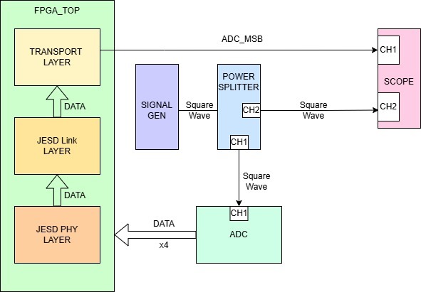
We planning to check the determinstic latency between JESD204B RX and ADC, I have a reference setup image we are planning to use for proving the deterministic latency. 

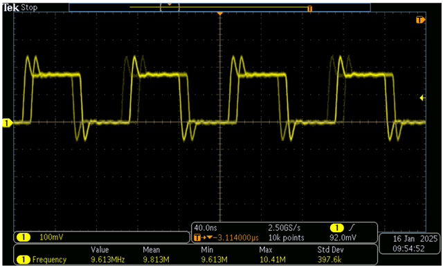
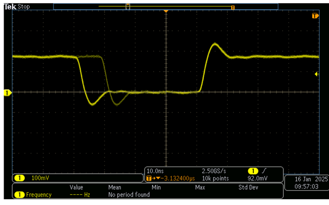
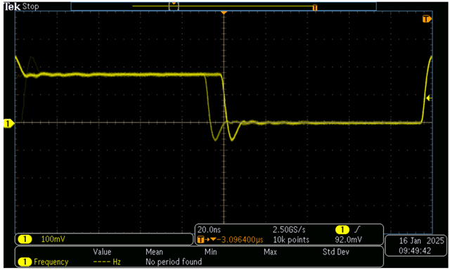
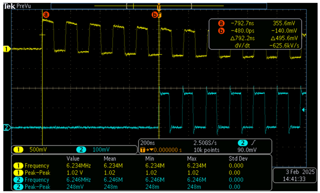
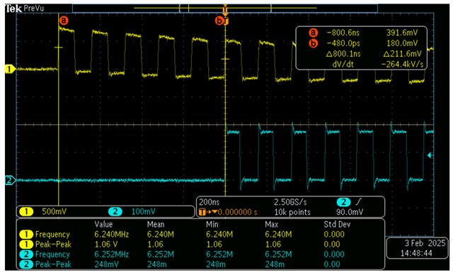
But we facing some issue with the ADC sample MSB bit, if we capture the ADC_MSB bit the duty cycle is not constant always, also the rising and falling edge have some overlapping. 
We are sending a sine wave as input to at different frequencies for testing but as we increase the frequency the overlapping increases. So can help us to debug this issue since if the duty is not constant we cannot say the signal is relaible for use to prove deterministic latency. I have attached the capture images at 5MHz.

5MHz 


  • Hi,

    Based on the jesd subclass type Sync/sysref  is used in JESD for alignment . But this signal gets latched on clock . Is your device clock , sync/sysref and signal you are generating are  locked ?  

  • Hi Sachin, 

    The signal we are generating is independent from sysref and device clock, we are using JESD6600 as the square wave generator instead of generating it through FPGA. 

  • Nitin,

    So you are comparing the MSB data from ADC with input signal ? Since clock and signal are not locked we need input signal reference to compare the ADC output data.

  • Hi Sachin, 

    Yes we are comparing the MSB data with ADC input signal 
    I have attached our setup for your reference 


    I am not getting why we need to synchronize the signal generator to the JESD clock, and how this is creating this duty cycle changes. 
    Also, by "Since clock and signal are not locked we need input signal reference to compare the ADC output data" this you mean that we need to put trigger on the ADC input. 

    I check the measurements with putting the trigger on the ADC input and then comparing it with ADC_MSB bit still the edges are not clean there is jitter on the edges. 


    So can you help us to debug this issue. 

  • If your clock and signal source is not locked run to run it can have phase variation. Or signal frequency can drift very slightly over time . So to avoid these kind of issue generally reference out (usually 10MHz) is taken from one source and given to ref in of other source . 

     So you need to do this for clock source and signal source . Once that is done you should see repeatable data .

  • Hi Sachin 

    Thanks for the input, we changed the source signal. Now we are generating the input signal from FPGA itself from same device clock and now we are not getting this this. 

    But, we are getting an another issue that when we measure the determinstic latency for the setup it remains almost constant but once in 5-6 power cycle we see a drift of 8ns. We are operating at 125MHz device clock, we changed the delay between the device clock and sysref from LMK but still we are getting this issue. Can you help us to debug this issue. I am attaching the scope waveform in both the cases for your reference. 

    with 8ns variation 

    without 8ns variation 

  • Hi, 

    Any update on this ?

  • Nitin,

    Sorry for the delay .

    I see that b pointer threshold  is different in these two picture . Am i missing something ?

    125MHz one clock cycle is 8ns . This is indicating 1 clock cycle miss. How is sysref generated for FPGA ?


  • Hi Sachin, 

    The pointer is set as per the blue waveform but the threshold reference it is taking from the upper waveform and intially the offset of input waveform is not zero due to power splitter in the path, so maybe due to that this threshold is coming negative 

    We are generating sysref, GTX clock, device clock and ADC sampling clock from the onboard LMK, I am using the following config file for the ADC eval board configuration 

    LMK04826|0x00 0x10
    LMK04826|0x02 0x00
    LMK04826|0x100 0x19 //GTX clk: div16 -
    LMK04826|0x101 0x00
    LMK04826|0x102 0x00
    LMK04826|0x103 0x00
    LMK04826|0x104 0x20
    LMK04826|0x105 0x00
    LMK04826|0x106 0xF0
    LMK04826|0x107 0x11
    LMK04826|0x108 0x05 //ADC-CLK: DCLK0 is div4, eventually div16
    LMK04826|0x109 0x00
    LMK04826|0x10A 0x00
    LMK04826|0x10B 0x00
    LMK04826|0x10C 0x20
    LMK04826|0x10D 0x00
    LMK04826|0x10E 0xF0
    LMK04826|0x10F 0x12
    LMK04826|0x110 0x00
    LMK04826|0x111 0x00
    LMK04826|0x112 0x00
    LMK04826|0x113 0x00
    LMK04826|0x114 0x20
    LMK04826|0x115 0x00
    LMK04826|0x116 0xF9
    LMK04826|0x117 0x44
    LMK04826|0x118 0x10
    LMK04826|0x119 0x00
    LMK04826|0x11A 0x00
    LMK04826|0x11B 0x00
    LMK04826|0x11C 0x20
    LMK04826|0x11D 0x00
    LMK04826|0x11E 0xF9
    LMK04826|0x11F 0x11
    LMK04826|0x120 0x14
    LMK04826|0x121 0x00
    LMK04826|0x122 0x00
    LMK04826|0x123 0x00
    LMK04826|0x124 0x20
    LMK04826|0x125 0x00
    LMK04826|0x126 0xF1
    LMK04826|0x127 0x11
    LMK04826|0x128 0x04
    LMK04826|0x129 0x55
    LMK04826|0x12A 0x00
    LMK04826|0x12B 0x00
    LMK04826|0x12C 0x20
    LMK04826|0x12D 0x00
    LMK04826|0x12E 0xF9
    LMK04826|0x12F 0x11
    LMK04826|0x130 0x02
    LMK04826|0x131 0x00
    LMK04826|0x132 0x00
    LMK04826|0x133 0x00
    LMK04826|0x134 0x20
    LMK04826|0x135 0x00
    LMK04826|0x136 0xF9
    LMK04826|0x137 0x01
    LMK04826|0x138 0x20 //VCO mux = VCO_0
    LMK04826|0x139 0x00 //Normal SYNC mode
    LMK04826|0x13A 0x02 //SYSREF_DIV[11:8]
    LMK04826|0x13B 0x80 //SYSREF_DIV[7:0]
    LMK04826|0x13C 0x00
    LMK04826|0x13D 0x08
    LMK04826|0x13E 0x00
    LMK04826|0x13F 0x06 //
    LMK04826|0x140 0x80
    LMK04826|0x141 0x00
    LMK04826|0x142 0x00
    LMK04826|0x143 0x11
    LMK04826|0x144 0xFF
    LMK04826|0x145 0x00
    LMK04826|0x146 0x12
    LMK04826|0x147 0x18
    LMK04826|0x148 0x10
    LMK04826|0x149 0x50
    LMK04826|0x14A 0x33
    LMK04826|0x14B 0x16
    LMK04826|0x14C 0x00
    LMK04826|0x14D 0x00
    LMK04826|0x14E 0x00
    LMK04826|0x14F 0x7F
    LMK04826|0x150 0x03
    LMK04826|0x151 0x02
    LMK04826|0x152 0x00
    LMK04826|0x153 0x00 //
    LMK04826|0x154 0x78
    LMK04826|0x155 0x00
    LMK04826|0x156 0x7D //CLKin1 R PLL1(forward divide) = 125
    LMK04826|0x157 0x00
    LMK04826|0x158 0x96
    LMK04826|0x159 0x00
    LMK04826|0x15A 0x64 //CLKin1 N PLL1(feedback divide) = 100
    LMK04826|0x15B 0xD4
    LMK04826|0x15C 0x20
    LMK04826|0x15D 0x00
    LMK04826|0x15E 0x00
    LMK04826|0x15F 0x0B
    LMK04826|0x160 0x00
    LMK04826|0x161 0x14 //PLL2 R (forward divide) = 20
    LMK04826|0x162 0x45 //PLL2 prescaler = 2, OSCin_FREQ = 63 - 127MHz, Doubler Enabled
    LMK04826|0x163 0x00
    LMK04826|0x164 0x00
    LMK04826|0x165 0x05
    LMK04826|0x166 0x00
    LMK04826|0x167 0x00
    LMK04826|0x168 0x7D //PLL2 N = 96(120MHz)
    LMK04826|0x169 0x59
    LMK04826|0x16A 0x20
    LMK04826|0x16B 0x00
    LMK04826|0x16C 0x00
    LMK04826|0x16D 0x00
    LMK04826|0x16E 0x13
    LMK04826|0x17C 0x01
    LMK04826|0x17D 0x0F
    LMK04826|0x145 0x7F // Added according to Datasheet recommendation
    LMK04826|0x171 0xAA // Added according to Datasheet recommendation
    LMK04826|0x172 0x02 // Added according to Datasheet recommendation
    LMK04826|0x139 0x00 //Normal SYNC mode
    LMK04826|0x144 0x00
    LMK04826|0x143 0x11
    LMK04826|0x143 0x31
    LMK04826|0x143 0x11
    LMK04826|0x144 0xFF
    LMK04826|0x143 0x13
    LMK04826|0x139 0x03 //Normal SYNC mode
    AFE58JD48_GLOBAL|0x12 0x000A // Control 16CH Enable common digital and JESD registers.
    AFE58JD48_GLOBAL|0x1E 0x0003 // Select all 16Chs
    AFE58JD48_Common_DIG|0x31 0x02C0 //PLL_MODE = 40X, CTRL_K=1, CTRL_MODE = 1
    AFE58JD48_Common_DIG|0x34 0x090F //JESD_SUBCLASS=1, JESD_VER=1, K=(15+1)
    AFE58JD48_Common_DIG|0x35 0x03C0 // L=(3+1), CTRL_L, CTRL_M
    AFE58JD48_Common_DIG|0x36 0x0007 // M=(7+1)
    AFE58JD48_Common_DIG|0x29 0x0000
    AFE58JD48_GLOBAL|0x12 0x0000 // Disable page
    AFE58JD48_VCA|0xC5 0x2A02
    AFE58JD48_VCA|0xC9 0x0000
    AFE58JD48_VCA|0xCA 0x0000
    AFE58JD48_VCA|0xCB 0x0000
    AFE58JD48_VCA|0xCC 0x0000
    AFE58JD48_VCA|0xCD 0x0000
    AFE58JD48_VCA|0xCE 0x8000
    AFE58JD48_VCA|0xCF 0x0000
    AFE58JD48_VCA|0xD0 0x0001
    AFE58JD48_VCA|0xDD 0x0200
    AFE58JD48_VCA|0xDE 0x00C3
    AFE58JD48_VCA|0xDF 0x0040
    AFE58JD48_VCA|0xE8 0x0000
    AFE58JD48_VCA|0xE9 0x0000
    AFE58JD48_VCA|0xEA 0x0000
    AFE58JD48_VCA|0xEB 0x0000
    AFE58JD48_VCA|0xEC 0x0000
    AFE58JD48_VCA|0xED 0x0000
    AFE58JD48_VCA|0xEE 0x0000
    AFE58JD48_VCA|0xEF 0x0000