This thread has been locked.

If you have a related question, please click the "Ask a related question" button in the top right corner. The newly created question will be automatically linked to this question.

AFE58JD48EVM: Query regarding deterministic latency one device clock cycle variation

Part Number: AFE58JD48EVM
Other Parts Discussed in Thread: LMK04826, AFE58JD48

Tool/software:

Hi, 

We are testing determistic latency for AFE58JD48EVM with JESD204B RX IP on EFINIX FPGA, I have attached the setup we are using for your reference. 

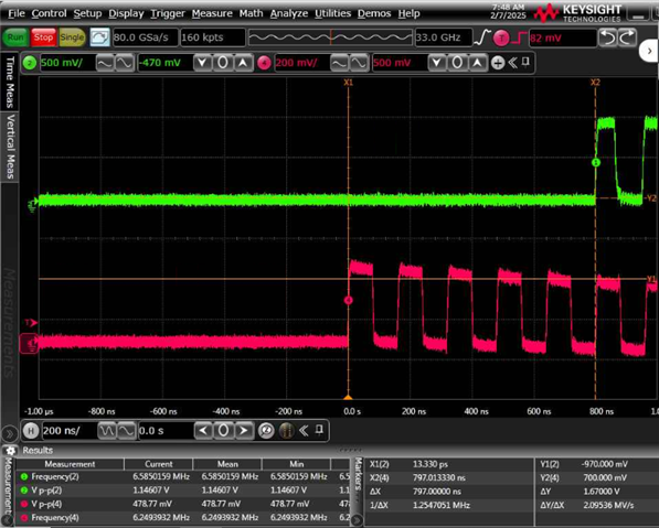
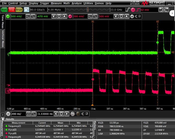
We are generating a 6.25MHz square wave from FPGA itself with device clock, LMK is used for both FPGA(device clock and SYSREF) and ADC (sampling clock and SYSREF) and we are operating at 5Gbps lane rate in 40X mode. FPGA is operating at 125Mhz device clock and ADC is also operating at 125MHz sampling clock(Genarting 500MHz from LMK since there is 1/4 buffer in path). We are creating 2 square waves from the square wave generated by FPGA using 1*2 splitter and one channel is being used as ADC input and other channel as reference for the scope to measure the total delay in the path. 

We did testing with this setup and did some measurements but in every 5-6 power cycle we are getting is variation of 8ns which is eual to our device clock period. Our total latency in the path is around 789ns and some times it comes out to be 797ns. Intially we doubted that there might be some issue with the sysref capturing in the JESDRX side but we tried with multiple clock delay options in the sysref path in the LMK side for both FPGA and ADC. But the results are not improving,  the total latency is changing but the 8ns variation is still coming. Then we analyze the captured results and I find out that the captured ADC MSB bit duty cycle is not constant always and it is taking some time to settle to 50% duty cycle. And when we are getting the 8ns variation the catured frequency is liitle change from the 6.25MHz, it is coming around 6.58MHz and if we calculate the period difference between the 6.58Mhz and 6.25MHz it comes out to be 8ns. So I am doubting this catured MSB bit frequency variation could be reason but not sure why this coming. So can you help us with this, is there anything we are missing from the ADC data capturing side. I have attached the captured results for your reference. 

  • Hi,

    Good case : 6.25 MHz with 5 cycle 

    latency expected is (1000/6.25)* 5 ns = 800ns (actual result : 797ns )

    Clock freq shift case: 6.585MHz

    latency expected is (1000/6.585)* 5 ns = 759ns


    But you are getting 789ns which is not matching .

    So I suspect it is still 1 clock cycle mismatch . 

    Can you change the trigger point to 20% of the max value and repeat the experiment ? If there is noise in the threshold detection point you can see this issue . Do you agree on this ?

  • Hi Sachin, 

    Yes noise can be a reason, but I changed the triggering to 20% of the max value, still same results I am getting.
    Also input square wave is 6.25MHz always its the ADC_MSB (green in colur) which is sometimes 6.585MHz. Is there any way to check if we are not meeting setup and hold time between sampling clock and sysref on the ADC side ? 

  • Nitin,

    Based on offset of the device and noise duty cycle can change .

    Can you please try enabling digital HPF in the device ? Datasheet section 10.3.7.3 Digital HPF and Gain explains how to enable this .

  • Hi Sachin, 

    Thanks for your quick response !

    I will check it out and share you the results. 

    Also to add I took some more measurements with just reseting the JESD RX IP and keeping the LMK and ADC config same, with this test case the variation of 8ns is not there. So I doubt that on power cycle the device clock to sysref delay is not constant and it is changing on every power cycle. 

    I have attached the register configuration I am using for ADC EVAL board, I am using divider reset method for device clock to sysref synchronization. 

    LMK04826|0x00 0x10
    LMK04826|0x02 0x00
    LMK04826|0x100 0x19 //GTX clk: div16 -
    LMK04826|0x101 0x00
    LMK04826|0x102 0x00
    LMK04826|0x103 0x00
    LMK04826|0x104 0x20
    LMK04826|0x105 0x00
    LMK04826|0x106 0xF0
    LMK04826|0x107 0x11
    LMK04826|0x108 0x05 //ADC-CLK: DCLK0 is div4, eventually div16
    LMK04826|0x109 0x00
    LMK04826|0x10A 0x00
    LMK04826|0x10B 0x00
    LMK04826|0x10C 0x20
    LMK04826|0x10D 0x00
    LMK04826|0x10E 0xF0
    LMK04826|0x10F 0x12
    LMK04826|0x110 0x00
    LMK04826|0x111 0x00
    LMK04826|0x112 0x00
    LMK04826|0x113 0x00
    LMK04826|0x114 0x20
    LMK04826|0x115 0x00
    LMK04826|0x116 0xF9
    LMK04826|0x117 0x44
    LMK04826|0x118 0x10
    LMK04826|0x119 0x00
    LMK04826|0x11A 0x00
    LMK04826|0x11B 0x00
    LMK04826|0x11C 0x20
    LMK04826|0x11D 0x00
    LMK04826|0x11E 0xF9
    LMK04826|0x11F 0x11
    LMK04826|0x120 0x14
    LMK04826|0x121 0x00
    LMK04826|0x122 0x00
    LMK04826|0x123 0x00
    LMK04826|0x124 0x20
    LMK04826|0x125 0x00
    LMK04826|0x126 0xF1
    LMK04826|0x127 0x11
    LMK04826|0x128 0x04
    LMK04826|0x129 0x55
    LMK04826|0x12A 0x00
    LMK04826|0x12B 0x00
    LMK04826|0x12C 0x20
    LMK04826|0x12D 0x00
    LMK04826|0x12E 0xF9
    LMK04826|0x12F 0x11
    LMK04826|0x130 0x02
    LMK04826|0x131 0x00
    LMK04826|0x132 0x00
    LMK04826|0x133 0x00
    LMK04826|0x134 0x20
    LMK04826|0x135 0x00
    LMK04826|0x136 0xF9
    LMK04826|0x137 0x01
    LMK04826|0x138 0x20 //VCO mux = VCO_0
    LMK04826|0x139 0x00 //Normal SYNC mode
    LMK04826|0x13A 0x02 //SYSREF_DIV[11:8]
    LMK04826|0x13B 0x80 //SYSREF_DIV[7:0]
    LMK04826|0x13C 0x00
    LMK04826|0x13D 0x08
    LMK04826|0x13E 0x00
    LMK04826|0x13F 0x06 //
    LMK04826|0x140 0x80
    LMK04826|0x141 0x00
    LMK04826|0x142 0x00
    LMK04826|0x143 0x11
    LMK04826|0x144 0xFF
    LMK04826|0x145 0x00
    LMK04826|0x146 0x12
    LMK04826|0x147 0x18
    LMK04826|0x148 0x10
    LMK04826|0x149 0x50
    LMK04826|0x14A 0x33
    LMK04826|0x14B 0x16
    LMK04826|0x14C 0x00
    LMK04826|0x14D 0x00
    LMK04826|0x14E 0x00
    LMK04826|0x14F 0x7F
    LMK04826|0x150 0x03
    LMK04826|0x151 0x02
    LMK04826|0x152 0x00
    LMK04826|0x153 0x00 //
    LMK04826|0x154 0x78
    LMK04826|0x155 0x00
    LMK04826|0x156 0x7D //CLKin1 R PLL1(forward divide) = 125
    LMK04826|0x157 0x00
    LMK04826|0x158 0x96
    LMK04826|0x159 0x00
    LMK04826|0x15A 0x64 //CLKin1 N PLL1(feedback divide) = 100
    LMK04826|0x15B 0xD4
    LMK04826|0x15C 0x20
    LMK04826|0x15D 0x00
    LMK04826|0x15E 0x00
    LMK04826|0x15F 0x0B
    LMK04826|0x160 0x00
    LMK04826|0x161 0x14 //PLL2 R (forward divide) = 20
    LMK04826|0x162 0x45 //PLL2 prescaler = 2, OSCin_FREQ = 63 - 127MHz, Doubler Enabled
    LMK04826|0x163 0x00
    LMK04826|0x164 0x00
    LMK04826|0x165 0x05
    LMK04826|0x166 0x00
    LMK04826|0x167 0x00
    LMK04826|0x168 0x7D //PLL2 N = 96(120MHz)
    LMK04826|0x169 0x59
    LMK04826|0x16A 0x20
    LMK04826|0x16B 0x00
    LMK04826|0x16C 0x00
    LMK04826|0x16D 0x00
    LMK04826|0x16E 0x13
    LMK04826|0x17C 0x01
    LMK04826|0x17D 0x0F
    LMK04826|0x145 0x7F // Added according to Datasheet recommendation
    LMK04826|0x171 0xAA // Added according to Datasheet recommendation
    LMK04826|0x172 0x02 // Added according to Datasheet recommendation
    LMK04826|0x139 0x00 //Normal SYNC mode
    LMK04826|0x144 0x00
    LMK04826|0x143 0x11
    LMK04826|0x143 0x31
    LMK04826|0x143 0x11
    LMK04826|0x144 0xFF
    LMK04826|0x143 0x13
    LMK04826|0x139 0x03 //Normal SYNC mode
    AFE58JD48_GLOBAL|0x12 0x000A // Control 16CH Enable common digital and JESD registers.
    AFE58JD48_GLOBAL|0x1E 0x0003 // Select all 16Chs
    AFE58JD48_Common_DIG|0x31 0x02C0 //PLL_MODE = 40X, CTRL_K=1, CTRL_MODE = 1
    AFE58JD48_Common_DIG|0x34 0x090F //JESD_SUBCLASS=1, JESD_VER=1, K=(15+1)
    AFE58JD48_Common_DIG|0x35 0x03C0 // L=(3+1), CTRL_L, CTRL_M
    AFE58JD48_Common_DIG|0x36 0x0007 // M=(7+1)
    AFE58JD48_Common_DIG|0x29 0x0000
    AFE58JD48_GLOBAL|0x12 0x0000 // Disable page
    AFE58JD48_VCA|0xC5 0x2A02
    AFE58JD48_VCA|0xC9 0x0000
    AFE58JD48_VCA|0xCA 0x0000
    AFE58JD48_VCA|0xCB 0x0000
    AFE58JD48_VCA|0xCC 0x0000
    AFE58JD48_VCA|0xCD 0x0000
    AFE58JD48_VCA|0xCE 0x8000
    AFE58JD48_VCA|0xCF 0x0000
    AFE58JD48_VCA|0xD0 0x0001
    AFE58JD48_VCA|0xDD 0x0200
    AFE58JD48_VCA|0xDE 0x00C3
    AFE58JD48_VCA|0xDF 0x0040
    AFE58JD48_VCA|0xE8 0x0000
    AFE58JD48_VCA|0xE9 0x0000
    AFE58JD48_VCA|0xEA 0x0000
    AFE58JD48_VCA|0xEB 0x0000
    AFE58JD48_VCA|0xEC 0x0000
    AFE58JD48_VCA|0xED 0x0000
    AFE58JD48_VCA|0xEE 0x0000
    AFE58JD48_VCA|0xEF 0x0000

    Also one more doubt that there is a buffer between LMK and ADC which is dividing the LMK clock by 4, so can that affect the legth matching between sampling clock to sysref, or can that create a one clock cycle latency. In my config I am generating a 500MHz clock from LMK and 125MHz is out ADC sampling clock.

  • Nitin,

    Good to  know that you are able to achieve repeatable data .

    Let me check whether in this EVM length matching is done or not. 

    I infer from your comment that power cycling was causing issue . Is it just device power cycling or EVM power cycling ?

  • Hi Sachin, 


    When we are powercycling both the complete EVM and also the FPGA, we are getting this issue. 

    Length matching can be an issue, also the divider is four as per current setting. So there will be four phase relationship possible between input clock and the output clock. That can also be a reason.

  • Nitin,

    Can you please try instead of power cycling just do a global power down to device and clear that bit and repeat the experiment ?

    This 1 clock error can be in AFE or receiver(FPGA) .